Ceramic Substrate Dielectric Breakdown Guide: Testing Principles, Weibull Statistics, and Defect Screening
Technical News
This ceramic substrate dielectric breakdown guide details the essential testing protocols and failure physics for high-power electronics. Ceramic substrates serve as the indispensable structural and electrical isolation backbone for high-power semiconductor electronics, electric vehicle (EV) traction inverters, wind power converters, and aerospace motor drives. While advanced substrate ceramics—such as alumina (Al2O3), aluminum nitride (AlN), and silicon nitride (Si3N4)—exhibit high thermal conductivity and room-temperature electrical insulation, their operational reliability depends strictly on their capacity to withstand severe electric field stress. High-voltage dielectric breakdown testing is the benchmark evaluation methodology used to determine the ultimate electrical withstand limits, dielectric strength, and partial discharge safety margins of metallized ceramic substrates.
In high-voltage direct bonded copper (DBC) and active metal brazing (AMB) assemblies, power switches operate under continuous DC-link bus potentials of 800V to several kilovolts with rapid switching transients (high dV/dt), necessitating distinct evaluation methodologies as explored in our ceramic substrate breakdown testing DC vs AC technology analysis. By systematically applying an escalating electric field across the ceramic barrier until an irreversible conductive breakdown path forms, materials engineers can quantify insulation safety margins, identify defect thresholds, and prevent catastrophic in-service component failure.
Fundamentals of Dielectric Breakdown in Ceramic Substrates
Dielectric breakdown in solid inorganic insulators represents the transition of an insulating ceramic into an irreversible conductor under high electrical field stress, governed by the electro-physical mechanisms detailed in our guide on ceramic voltage breakdown testing principles and factors. In pristine crystalline lattices, intrinsic breakdown occurs when the applied electric field accelerates free electrons to kinetic energies sufficient to ionize valence electrons through collision cascades.
In industrial ceramic substrates, dielectric failure is predominantly governed by extrinsic microstructural imperfections and localized electric field concentrations:
- Micro-porosity and Sintering Voids: Air pockets and sub-surface pores exhibit lower relative permittivity (
ε_pore ≈ 1.0) than the dense bulk ceramic matrix (ε_ceramic ≈ 8 to 10). This dielectric mismatch crowds electric flux into the voids, triggering localized partial discharges at field levels far below theoretical lattice limits. - Copper Etch Edge Electric Field Crowding: In DBC and AMB substrates, the chemical etching of thick copper foils leaves sharp peripheral edge profiles. These sharp metallization contours act as localized field concentrators, elevating the local electric field by factors of 3 to 8 over the nominal average field.
- Microcracks and Grain Boundary Inhomogeneities: Thermal expansion mismatches between bonded copper foils and the underlying ceramic introduce mechanical shear stresses during thermal cycling, producing micro-fissures where local dielectric fatigue initiates.
- Secondary Phase Impurities: Segregated glassy phases, unreacted sintering fluxes, or metallic inclusions along grain boundaries lower the localized activation energy for electrical treeing.
Benchmark of DBC and AMB Power Electronic Ceramic Substrates
Selecting substrate materials for high-voltage power modules requires balancing dielectric breakdown strength, thermal conductivity, mechanical bending strength, and partial discharge endurance.
| Ceramic Substrate Technology | Ceramic Formulation | Ceramic Thickness (mm) | Copper Foil Thickness (mm) | DC Breakdown Voltage (kV) | Dielectric Strength (kV/mm) | Partial Discharge Extinction Voltage (kV AC) | Thermal Conductivity k (W/m·K) | Primary Power Electronics Application |
|---|---|---|---|---|---|---|---|---|
| Al2O3 DBC | 96% Standard Alumina | 0.38 | 0.30 | 14.0 - 18.0 | 35 - 45 | 1.8 - 2.4 | 24 | Standard 650V/1200V IGBT industrial motor drives |
| Al2O3 DBC (Thick) | 96% Standard Alumina | 0.63 | 0.30 | 22.0 - 28.0 | 32 - 42 | 2.6 - 3.2 | 24 | High-voltage industrial power supplies, solar inverters |
| AlN DBC | High Thermal Purity AlN | 0.63 | 0.30 | 18.0 - 24.0 | 28 - 36 | 2.2 - 2.8 | 170 - 180 | High-power density wind power modules, rail traction |
| Si3N4 AMB | High Toughness Silicon Nitride | 0.32 | 0.50 - 0.80 | 16.0 - 22.0 | 50 - 68 | 2.8 - 3.6 | 85 - 90 | 800V/1200V Silicon Carbide (SiC) EV traction inverters |
| Si3N4 AMB (Thin) | Ultra-Thin High Conductivity | 0.25 | 0.50 | 14.0 - 18.0 | 55 - 72 | 2.4 - 3.0 | 90 | Next-generation compact SiC automotive drivetrains |
| ZTA DBC | Zirconia Toughened Alumina | 0.38 | 0.30 | 16.0 - 20.0 | 40 - 50 | 2.0 - 2.6 | 26 | High-vibration industrial drives, automotive auxiliaries |
Silicon nitride AMB substrates deliver the highest dielectric breakdown strength (exceeding 50 to 70 kV/mm) and exceptional fracture toughness. This combination enables the use of thinner ceramic layers (0.25 to 0.32 mm) with thicker copper foils (up to 0.8 mm), drastically reducing thermal resistance while sustaining high dielectric withstand margins.
Dielectric Puncture vs Surface Flashover Troubleshooting
Accurate breakdown evaluation requires rigorously distinguishing true bulk ceramic puncture from superficial surface tracking arcs or ambient flashover.
| Diagnostic Observation | Physical Failure Mode | Microscopic Root Cause | Corrective Testing Protocol |
|---|---|---|---|
| Puncture hole located at copper foil etch edge | True bulk dielectric breakdown | Electric field crowding at sharp copper etch step exceeding ceramic puncture strength | Optimize chemical etch pull-back margin; chamfer copper edge radius; verify oil immersion |
| Superficial tracking arc along substrate perimeter | Surface flashover | Ambient gas ionization or surface contamination bridging top and bottom metallization | Submerge substrate completely in degassed silicone oil; increase edge clearance margin (≥ 2.0 mm) |
| Micro-crack shattering without melted crater | Electromechanical mechanical fracture | Anisotropic thermal-piezoelectric stress from rapid high-voltage step application | Reduce voltage ramp rate (< 500 V/s); utilize spring-loaded electrodes with controlled clamp force |
| Continuous micro-current bubbling in oil bath | Pre-breakdown partial discharge | Entrapped moisture or micro-voids in liquid dielectric or ceramic grain boundaries | Degas and dry silicone oil; bake ceramic substrates at 120°C for 2 hours prior to immersion |
True dielectric breakdown punches a permanent, physical hole through the ceramic volume, often surrounded by localized molten material. Surface flashover leaves superficial soot marks without degrading the internal bulk volume.
Mathematical Models of Ceramic Breakdown Scaling
The dielectric breakdown strength of ceramic substrates is not a constant material property; it scales with specimen thickness and voltage ramp rate according to statistical defect models:
- Thickness Scaling Power Law: Due to volumetric defect distribution statistics, thicker ceramic plates exhibit lower apparent dielectric strength than thin sheets:
V_bd = V_0 * ( d )^n
E_bd = V_bd / d = V_0 * ( d )^( n - 1 )
where V_bd is breakdown voltage, d is thickness, and n is an empirical scaling exponent (typically between 0.5 and 0.8 for polycrystalline ceramics, as also observed in piezoelectric ceramics voltage breakdown testing guide). Consequently, doubling substrate thickness does not double its breakdown voltage.
- Voltage Ramp Rate Dependence: Conforming to ASTM D149, dielectric breakdown voltage depends on the rate of voltage increase (
dV/dt):
V_bd(ramp) = V_ref * [ ( dV / dt ) / r_0 ]^m
where r_0 is a baseline reference ramp rate (e.g., 500 V/s) and m is an empirical factor reflecting thermal relaxation. Fast ramp rates capture short-term dielectric strength, whereas slow rates permit thermal accumulation and dielectric fatigue.
High-Voltage Breakdown Characterization with MatMeas VBT-30KV
Evaluating the dielectric withstand performance of DBC and AMB substrates requires instrumentation combining wide voltage ranges, programmable ramp profiles, and microsecond arc suppression.
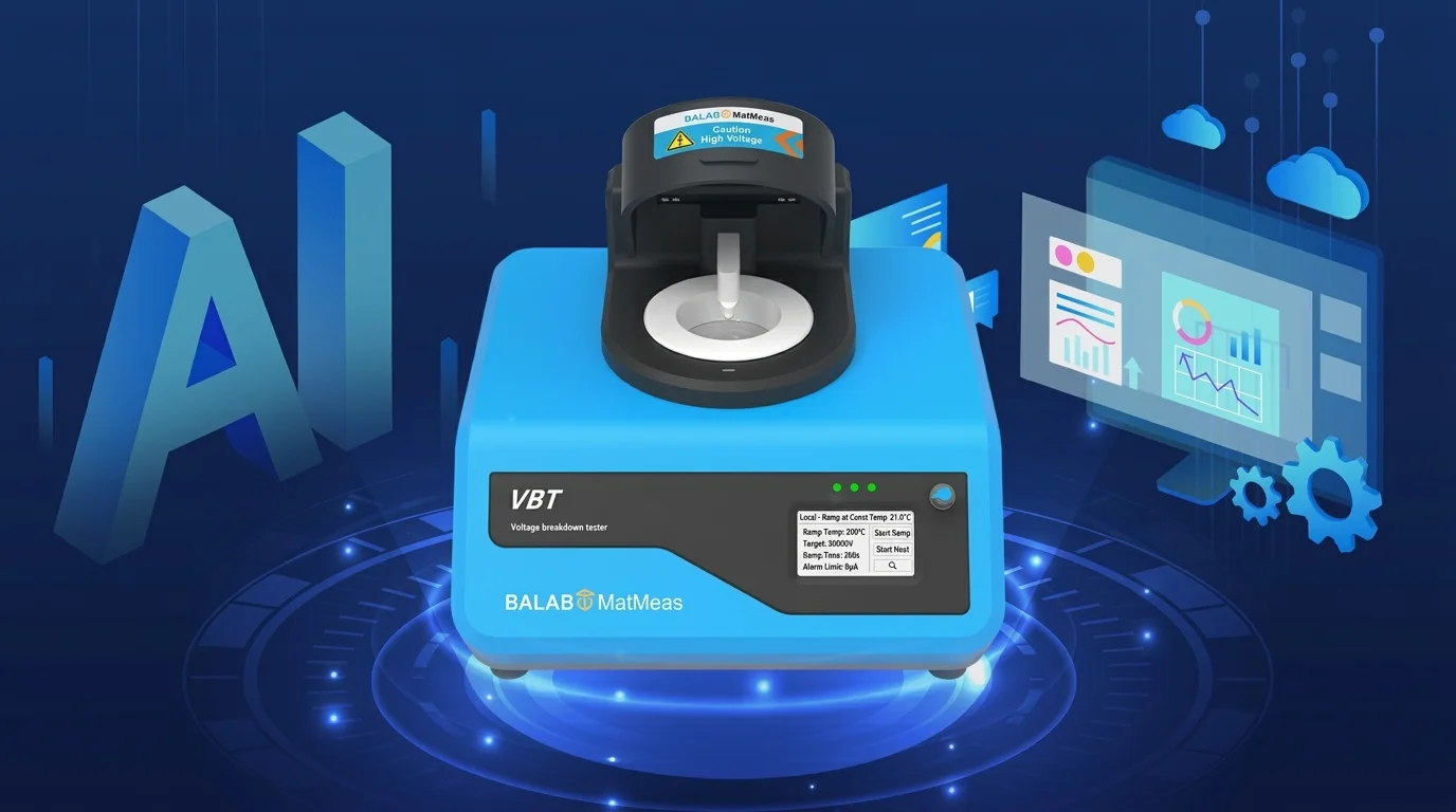
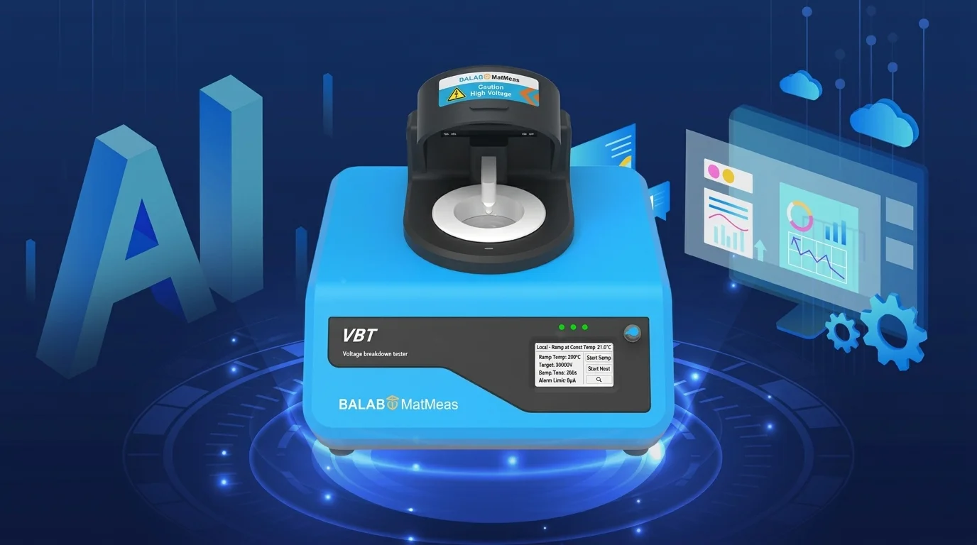
The MatMeas VBT-30KV Voltage Breakdown Tester is engineered for dielectric strength evaluation of technical ceramics, power substrates, and high-voltage insulation materials.
Key technical specifications of the VBT-30KV include:
- Digital High-Voltage Generation (0 to 30 kV): Continuously adjustable DC or AC output with programmable linear ramp rates (<5 kV/s) and fine step resolution.
- Integrated Silicone Oil Bath Fixture: Features an integrated oil bath testing chamber that suppresses peripheral edge flashover, ensuring all breakdown readings represent intrinsic bulk ceramic properties.
- Thermal Chamber Simulation (Ambient to 180°C): Integrated PID temperature regulation enables testing from room temperature up to 180°C, simulating real automotive power module operating conditions.
- Fast Microsecond Interlock Protection: Fast current-sensing hardware shuts off high voltage within microseconds upon current threshold breach (adjustable from 10 μA to 20 mA), preserving puncture craters for SEM failure analysis.
- Operator Safety Architecture: Dual safety interlocks, automatic high-voltage discharge grounding, and a shielded acrylic enclosure ensure complete operator safety during 30 kV procedures.
Frequently Asked Questions
How does surface flashover differ from true dielectric breakdown in ceramic substrates?
Surface flashover occurs when intense electric fields ionize ambient air or gas along the edges of the ceramic specimen, creating an external tracking spark without damaging the internal ceramic body. In contrast, true dielectric breakdown punches a permanent conductive hole directly through the ceramic bulk thickness, resulting in irreversible short-circuiting. To eliminate false flashover readings, testing must be conducted within a high-dielectric-strength silicone oil bath.
What voltage ramp rates are recommended for testing ceramic substrates?
Standardized testing protocols, including ASTM D149 and IEC 60243-1, recommend uniform linear ramp rates between 100 V/s and 1000 V/s (typically 500 V/s). Abrupt voltage surges can induce capacitive charging spikes and mechanical shock that trigger premature false failures. The MatMeas VBT-30KV provides programmable digital voltage ramps to ensure reproducible, traceable breakdown data.
Why do Si3N4 AMB substrates exhibit higher dielectric strength than Al2O3 DBC substrates?
Silicon nitride (Si3N4) possesses a fine-grained, interlocking microstructure with superior mechanical fracture toughness (6 to 8 MPa·m^0.5 compared to 3 to 4 MPa·m^0.5 for alumina). This dense microstructure resists electron avalanche propagation and localized thermal cracking, yielding intrinsic dielectric strengths exceeding 50 to 70 kV/mm, compared to 35 to 45 kV/mm for standard 96% alumina.
Request High-Precision Testing Solutions
Get expert guidance and customized instruments for your functional materials project.