Dielectric Breakdown Testing of Ceramic Substrates: DC vs. AC Technology
Technical News
Dielectric breakdown testing determines the limiting electrical stress at which a solid ceramic substrate transitions from a near-perfect electrical insulator to an ionized, conductive plasma puncture channel. In modern wide-bandgap (SiC and GaN) power modules, high-voltage direct-current (HVDC) converter stations, electric vehicle (EV) traction inverters, and high-frequency power supplies, ceramic substrates—principally high-purity alumina (Al2O3), aluminum nitride (AlN), and silicon nitride (Si3N4)—are subjected to relentless electrical stress.
A frequent and hazardous misconception among design engineers is assuming that a substrate's dielectric breakdown voltage (V_b) or dielectric breakdown strength (E_b = V_b / d, expressed in kV/mm) is a single, interchangeable physical constant that applies equally to direct-current (DC) and alternating-current (AC) working conditions.
In reality, the physical mechanisms that drive dielectric failure under DC electric fields are fundamentally different from those that operate under power-frequency or high-frequency AC fields. Under identical geometry, electrode configuration, and temperature, a technical ceramic substrate will typically fail under AC excitation at electric fields that are 30% to 60% lower than its DC breakdown threshold. Treating DC and AC dielectric strength values as interchangeable risks disastrous in-service insulation puncture, catastrophic short-circuit flashover, and module destruction.
To establish defensible qualification protocols adhering to ASTM D149, IEC 60243-1 (AC), and IEC 60243-2 (DC), testing laboratories must master the physical divergence between DC and AC breakdown, apply two-parameter Weibull statistical models, and enforce proper fluid immersion techniques.
Physical Divergence: DC Steady-State vs. AC Alternating Field Breakdown
The metrological divide between DC and AC breakdown originates in how the electric field distributes across the heterogeneous microstructure of the ceramic, and how electrical energy is converted into heat.
1. Electric Field Distribution: Resistivity Governing vs. Permittivity Governing
Polycrystalline ceramics are heterogeneous composites consisting of crystalline grains, amorphous intergranular glassy phases, and residual micro-porosity:
-
Under DC Steady-State Fields (Resistivity Control): Once initial capacitive charging currents decay, the steady-state electric field distribution is dictated strictly by the local direct-current electrical resistivity rho(r) of each microstructural phase, satisfying the continuity equation:
div(J) = 0 => div(E / rho) = 0
In a multi-phase ceramic, the electric field concentrates disproportionately in the regions of highest electrical resistivity (the crystalline grain interiors). Furthermore, continuous unipolar DC stress drives slow, irreversible ionic drift and carrier injection from the metallic electrodes. This leads to the accumulation of localized space charge pockets at grain boundaries and metal-ceramic interfaces, distorting the internal electric field and creating localized field enhancement spikes that trigger premature electronic avalanche.
-
Under AC Alternating Fields (Permittivity Control): Under sinusoidal AC excitation (E(t) = E_peak * sin(omega * t)), the electric field distribution is dictated strictly by the relative dielectric permittivity (dielectric constant, epsilon_r) of each phase, governed by the displacement continuity relation:
div(D) = 0 => div(epsilon_0 * epsilon_r * E) = 0
Under AC stress, the electric field concentrates intensely in regions possessing the lowest dielectric permittivity. In sintered ceramics, the lowest-permittivity phase is microscopic air/gas-filled pores (where epsilon_pore approx 1.0, compared to epsilon_ceramic approx 9 to 10 for alumina or AlN). Consequently, the electric field within an internal pore is magnified:
E_pore approx [3 * epsilon_ceramic / (2 * epsilon_ceramic + 1)] * E_applied
This electric field amplification ignites continuous partial discharge (PD) inside micro-pores at relatively low applied voltages.
2. Dielectric Loss Dissipation and Thermal Breakdown Acceleration
The most profound operational difference between DC and AC stress is internal dielectric self-heating:
-
Under DC Voltage: Ohmic Joule heating per unit volume W_in(DC) is governed solely by the minute bulk DC electrical conductivity sigma_dc:
W_in(DC) = sigma_dc * E_dc^2
Because high-purity ceramics exhibit volume resistivities exceeding 10^13 ohm*cm at room temperature (sigma_dc < 10^-11 S/m), DC Joule heating is practically negligible below 150 C.
-
Under AC Voltage: In addition to ohmic conduction, alternating fields continuously rotate defect dipoles and displace interfacial space charges back and forth every half-cycle. This dielectric dissipation produces massive volumetric self-heating W_in(AC):
W_in(AC) = omega * epsilon_0 * epsilon_r * tan(delta) * E_rms^2 = 2 * pi * f * epsilon_0 * epsilon_r * tan(delta) * (E_peak / sqrt(2))^2
Where omega is the angular frequency (2 * pi * f), tan delta is the dielectric loss tangent, and E_rms is the root-mean-square electric field.
Because AC dielectric loss heating scales directly with frequency f and the square of electric field, internal heat generation is several orders of magnitude higher under AC stress than under DC. Under continuous AC excitation, heat accumulates faster than it can conduct away through the metal electrodes, triggering the classical Wagner thermal runaway instability at substantially lower applied electric fields.
Comprehensive Comparison Matrix: DC vs. AC Dielectric Breakdown
The fundamental physical, electrical, and operational differences between DC and AC breakdown testing in technical ceramics are detailed in the table below.
| Metrological Parameter | Direct-Current (DC) Breakdown Testing | Alternating-Current (AC, 50/60 Hz) Breakdown Testing |
|---|---|---|
| Governing Material Property | Bulk volume resistivity distribution rho(T) and defect hopping | Relative dielectric permittivity distribution epsilon_r(omega) |
| Internal Field Concentration | Concentrates in high-resistivity grain interiors and depletion zones | Concentrates in low-permittivity voids, sintering pores, and micro-cracks |
| Peak-to-RMS Voltage Ratio | Peak voltage equals nominal DC voltage (V_peak = V_dc) | Peak voltage is 1.414 times nominal RMS voltage (V_peak = sqrt(2) * V_rms) |
| Dielectric Loss Self-Heating | Negligible at ambient temperatures; W_dc = sigma_dc * E^2 | Severe; W_ac = 2 * pi * f * epsilon_0 * epsilon_r * tan(delta) * E_rms^2 |
| Partial Discharge (PD) Activity | Occurs only transiently during voltage ramp; quenches at DC steady state | Ignites repeatedly every half-cycle (100 to 120 PD bursts per second at 50/60 Hz) |
| Space Charge Trapping | High; unipolar injection creates persistent internal polarization fields | Minimal; polarity reversal every half-cycle prevents persistent space-charge accumulation |
| Typical Breakdown Field Ratio | Baseline reference: 100% (e.g., 25 kV/mm DC for 96% alumina) | Significantly lower: E_ac(RMS) is typically 40% to 60% of E_dc |
| Primary International Standard | IEC 60243-2, ASTM D149 (Method B) | IEC 60243-1, ASTM D149 (Method A) |
| Primary In-Service Failure Mode | Electrostatic overstress puncture, space-charge-induced tracking | Wagner thermal runaway, partial discharge treeing, cyclic fatigue |
Statistical Modeling: Two-Parameter Weibull Distribution Analysis
Dielectric breakdown in brittle, polycrystalline ceramics is fundamentally a weakest-link statistical event. Sintered substrates contain a random spatial distribution of microstructural flaws—residual sintering pores, intergranular micro-cracks, and segregated glassy inclusions. Puncture invariably initiates at the single most severe defect within the stressed electrode volume.
Consequently, reporting a simple arithmetic mean of three or four breakdown tests is scientifically invalid. Standards such as IEEE Std 930 mandate testing a cohort of at least 15 to 20 identical specimens and fitting the failure fields E_b to a two-parameter Weibull distribution:
P_f(E) = 1 - exp[ - (E / E_0)^beta ]
Taking the natural logarithm twice yields the linear regression formulation:
ln[ -ln(1 - P_f) ] = beta * ln(E) - beta * ln(E_0)
Where:
-
P_f: The cumulative failure probability, estimated for the i-th ranked specimen (sorted in ascending order of breakdown strength) using the standard median rank formula:
P_f(i) = (i - 0.3) / (N + 0.4)
Where N is the total number of tested specimens.
-
E_0: The characteristic breakdown strength (scale parameter), corresponding to the electric field at which exactly 63.2% of the specimen cohort has failed.
-
beta: The Weibull modulus (shape parameter), represented by the slope of the linearized regression line.
A high Weibull modulus (beta >= 15 to 25) indicates superior microstructural uniformity, narrow pore size distributions, and highly repeatable manufacturing. Conversely, a low Weibull modulus (beta <= 5 to 8) indicates erratic defect populations, warning power module designers that the safe working field must be de-rated substantially below E_0 to prevent infant mortality failures.
Material Benchmark Comparison: Ceramic Substrate Breakdown Parameters
The table below provides experimentally verified DC and AC breakdown strengths, Weibull shape parameters, and typical AC-to-DC ratios across leading electronic ceramic substrates tested in dielectric oil.
| Ceramic Substrate Material | Typical Purity & Forming Method | Specimen Thickness (mm) | Characteristic DC Strength E_0(DC) (kV/mm) | Characteristic AC Strength E_0(AC, RMS) (kV/mm) | AC-to-DC Ratio (E_AC / E_DC) | Weibull Modulus beta (DC) | Weibull Modulus beta (AC) | Dominant Defect Limiting Strength |
|---|---|---|---|---|---|---|---|---|
| Alumina 96% (Al2O3) | 96% tape-cast + silicate fluxes | 0.635 mm | 22.5 to 26.0 | 12.0 to 14.5 | 0.53 to 0.56 | 12.5 | 9.8 | Intergranular silicate glass pores; secondary phase interfaces |
| High-Purity Alumina 99.8% | 99.8% fine-grained (sub-micron) | 0.500 mm | 32.0 to 38.0 | 18.5 to 22.0 | 0.58 to 0.60 | 18.2 | 14.5 | Residual sub-micron sintering micro-voids (< 1 um) |
| Aluminum Nitride (AlN) | >99% AlN + Y2O3 sintering aid | 0.635 mm | 24.0 to 28.0 | 13.5 to 16.0 | 0.56 to 0.58 | 14.0 | 10.5 | Second-phase yttrium aluminate inclusions; boundary thermal stress |
| Gas-Pressure Sintered Si3N4 | beta-Si3N4 with Al2O3/Y2O3 aids | 0.320 mm | 34.0 to 42.0 | 21.0 to 26.5 | 0.62 to 0.65 | 22.0 | 16.8 | Highly uniform interlocking grain matrix; high fracture toughness |
| LTCC Glass-Ceramic | Borosilicate crystallized matrix | 0.400 mm | 18.0 to 22.0 | 9.5 to 11.5 | 0.52 to 0.55 | 8.5 | 6.2 | Amorphous glass softening; open porosity in unconstrained sintered tapes |
| High-Purity Fused Silica | Amorphous 99.99% SiO2 | 1.000 mm | 50.0 to 65.0 | 32.0 to 40.0 | 0.62 to 0.64 | 25.0 | 20.5 | Intrinsic electronic avalanche; near-zero microstructural porosity |
Surface Flashover Suppression: The Vital Role of Shielded Oil Bath Testing
A frequent laboratory error when measuring ceramic dielectric strength is attempting to execute tests in an ambient air environment.
At standard temperature and pressure, dry air exhibits a dielectric breakdown strength of merely 3.0 kV/mm. When applying high voltages (e.g., 10 kV to 30 kV) across a 0.5 mm or 1.0 mm ceramic substrate in air, the intense electric field concentration at the triple junction (where the metallic electrode edge, the ceramic surface, and surrounding air meet) ionizes ambient nitrogen and oxygen molecules. This triggers immediate surface flashover—a violent, luminous electrical arc that wraps around the exterior edge of the substrate long before the electric field can penetrate and puncture the ceramic thickness. Testing in air measures only the surface creepage distance and atmospheric humidity, providing zero information about the material's bulk dielectric strength.
To suppress surface flashover and force the electrical stress into the bulk volume, ASTM D149 and IEC 60243 mandate submerging the test fixture and substrate in a high-dielectric-strength liquid medium—most commonly high-purity electrical insulating silicone oil or transformer oil (dielectric strength > 25 kV/mm to 35 kV/mm).
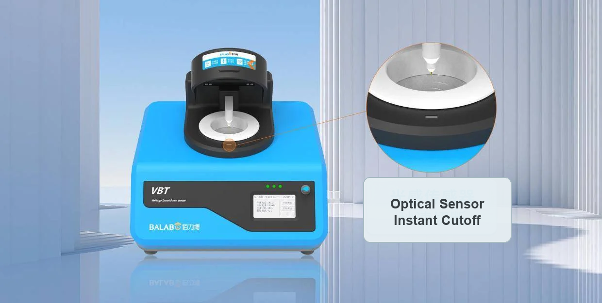
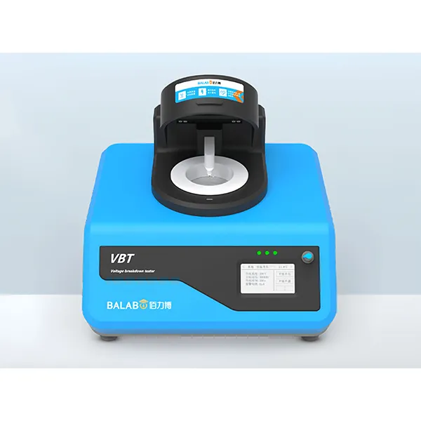
The MatMeas VBT-30KV Voltage Breakdown Tester provides a dedicated hardware platform engineered specifically to resolve this challenge. Equipped with a precision digital 30 kV high-voltage supply, the VBT-30KV incorporates an integrated temperature-controlled silicone oil bath operating from ambient room temperature up to +180 C. This allows engineers to eliminate surface flashover while simultaneously mapping the temperature-dependent breakdown curves of ceramic substrates across realistic power inverter operating temperatures.
Furthermore, a 30 kV dielectric breakdown releases substantial explosive plasma energy that can easily destroy delicate measurement electronics. The VBT-30KV incorporates an ultrafast optical and electronic trip-relay isolation circuit that clamps the high-voltage supply within microseconds of specimen puncture, preserving the microstructural puncture channel for post-mortem scanning electron microscopy (SEM) failure analysis while guaranteeing complete operator safety through heavy Faraday cage shielding and dual-circuit safety interlocks.
Standardized Step-by-Step SOP for DC and AC Breakdown Testing
To obtain standardized, statistically valid dielectric breakdown data complying with ASTM D149, IEC 60243-1, and IEC 60243-2, testing technicians should enforce this experimental protocol:
Step 1: Specimen Preparation and Cleaning
- Cut or machine ceramic substrate specimens into uniform square plates (recommended: 50 mm x 50 mm) or circular discs with thickness d between 0.3 mm and 1.0 mm. Ensure opposing faces are parallel to within +/-0.005 mm.
- Measure the exact thickness d at five distributed points within the central test zone using a calibrated spherical-anvil digital micrometer (+/-0.001 mm accuracy); record the minimum thickness d_min.
- Clean the specimen in an ultrasonic bath using acetone for 10 minutes, followed by 10 minutes in electronic-grade isopropanol. Bake at 150 C for 2 hours to eliminate all surface moisture films, then cool inside a desiccator.
Step 2: Electrode Alignment and Oil Bath Immersion
- Mount opposing polished brass or stainless steel spherical/cylindrical electrodes complying with ASTM D149 Table 1 (standard: unequal opposing cylinders, 25 mm diameter upper electrode and 75 mm diameter lower plate, with 2.5 mm edge radii).
- Position the ceramic substrate centrally between the electrodes, applying a calibrated mechanical clamping load (typically 1 N to 3 N) to ensure intimate contact without mechanical micro-cracking.
- Submerge the fixture assembly into the VBT-30KV silicone oil bath. Allow 15 minutes for oil degassing and thermal stabilization at the target temperature setpoint (e.g., 25 C or 150 C).
Step 3: Voltage Ramping and Failure Detection
- Mode Selection: Select either DC Mode (IEC 60243-2) or AC 50/60 Hz Mode (IEC 60243-1).
- Short-Time Ramp Test: Set the digital high-voltage controller to ramp linearly at a standardized rise rate of 500 V/s (or 1000 V/s) until puncture occurs.
- Trip Criterion: Program the trip sensitivity to 1.0 mA. Upon specimen puncture, the high-speed isolation relay clamps output voltage within microseconds, recording the peak breakdown voltage V_b.
- Calculate the dielectric breakdown strength: E_b = V_b / d_min.
Step 4: Weibull Parameter Fitting
- Repeat the breakdown test across a cohort of at least 15 to 20 identical specimens under identical conditions.
- Sort the recorded breakdown fields E_b in ascending order and compute median rank probabilities P_f(i).
- Plot ln[-ln(1 - P_f)] versus ln(E_b) to generate the linear Weibull plot.
- Extract the characteristic breakdown strength E_0 (at 63.2% failure probability) and the Weibull modulus beta from the slope.
Frequently Asked Questions (FAQ)
Why is the AC dielectric breakdown strength of a ceramic substrate consistently lower than its DC breakdown strength?
AC excitation induces two destructive mechanisms that are absent or negligible under DC stress: first, continuous alternating fields generate cyclic partial discharge (PD) inside microscopic sintering pores every half-cycle, rapidly eroding the surrounding ceramic. Second, AC dielectric loss (proportional to omega * epsilon_r * tan delta * E^2) generates substantial volumetric heat within the ceramic, accelerating Wagner thermal runaway at electric fields 30% to 60% lower than the DC threshold.
Why is testing in a temperature-controlled silicone oil bath mandatory for ceramic substrates?
The dielectric breakdown strength of air is only ~3 kV/mm. When applying high voltages across a thin ceramic substrate in air, the intense electric field concentration at the electrode edges ionizes air molecules, triggering surface flashover arcing across the perimeter long before the electric field punctures the bulk ceramic. Submerging the specimen in insulating silicone oil (strength > 25 kV/mm) suppresses air ionization and forces the electric field into the ceramic volume.
What is the engineering significance of the Weibull modulus beta in dielectric breakdown data?
The Weibull modulus beta represents the slope of the failure probability distribution and quantifies the microstructural uniformity of the ceramic. A high beta value (beta > 15) indicates uniform grain sizes, narrow pore distributions, and consistent manufacturing quality. A low beta value (beta < 8) signals widespread, erratic defects, requiring power module designers to impose a much larger safety de-rating margin.
How does the VBT-30KV protect against explosive energy release during a 30 kV dielectric puncture?
When a solid ceramic punctures at 30 kV, the sudden short circuit discharges significant stored capacitive energy, creating violent plasma arcing and electromagnetic surges. The VBT-30KV integrates an ultrafast optical and electronic trip sensor that detects discharge current within microseconds and isolates the high-voltage generator through dedicated dump circuits. This shields the internal electrometer from damage, preserves the ceramic failure channel for SEM analysis, and ensures complete operator safety.
Request High-Precision Testing Solutions
Get expert guidance and customized instruments for your functional materials project.