Measuring the Relative Permittivity of Ceramic Substrates
Technical News
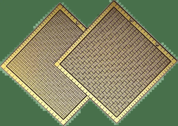
Ceramic substrates represent the physical and dielectric backbone of modern high-power electronics, advanced RF front-end modules, radar transceivers, and high-density multi-chip packaging. Materials such as high-purity alumina (Al2O3), aluminum nitride (AlN), silicon nitride (Si3N4), low-temperature co-fired ceramics (LTCC), and beryllium oxide (BeO) are selected for their distinct combinations of thermal conductivity, dielectric isolation, mechanical stiffness, and controlled permittivity. In high-frequency microstrip circuits and power semiconductor modules (such as SiC MOSFET and GaN HEMT power assemblies), the relative permittivity (real dielectric constant, epsilon_r') and dielectric loss tangent (tan delta) govern the characteristic impedance (Z0), phase velocity (v_p), electromagnetic propagation delay (t_pd), inter-trace crosstalk coupling, and overall volumetric power dissipation.
The propagation delay along a microstrip trace deposited on a non-magnetic ceramic dielectric is directly coupled to its effective relative permittivity:
t_pd = sqrt(epsilon_eff) / c
Where c represents the speed of light in vacuum (approximately 2.998e8 m/s), and epsilon_eff is the effective relative permittivity determined by the substrate permittivity, trace geometry, and electromagnetic fringe field distribution into the air. Similarly, the dielectric attenuation factor (alpha_d) in nepers per unit length increases linearly with frequency and dielectric loss:
alpha_d approx (pi * f / c) * sqrt(epsilon_eff) * tan(delta)
Because relative permittivity is intrinsically dependent on frequency, operational temperature, crystalline microstructure, and ambient atmospheric conditions, selecting and executing the correct metrological protocol is critical. A measurement technique optimized for kilohertz audio filters will fail completely at millimeter-wave radar bands, while microwave cavity perturbation methods cannot capture low-frequency space-charge relaxations or thermal phase transitions.
Dielectric Polarization Mechanisms and Frequency Dispersion
The dielectric response of inorganic polycrystalline ceramics arises from the superposition of four fundamental microscopic polarization mechanisms, each possessing a characteristic physical time constant and frequency cut-off:
- Space Charge and Interfacial (Maxwell-Wagner) Polarization: Dominant below 10 kHz and at elevated temperatures. Charge carriers (such as oxygen vacancies, lattice defects, and mobile alkali impurities) migrate across grain interiors and accumulate at grain boundaries or ceramic-electrode interfaces, forming localized potential barriers. This mechanism induces enormous apparent permittivity at low frequencies accompanied by high dielectric loss.
- Dipolar (Orientation) Polarization: Active from sub-hertz frequencies up to the low microwave regime (10^8 to 10^10 Hz). Permanent or defect dipoles (e.g., acceptor-oxygen vacancy defect complexes) reorient under the alternating electric field. As the excitation frequency approaches the relaxation frequency (f_r = 1 / (2 * pi * tau)), phase lag between the excitation and displacement vectors produces a distinct Debye-type dielectric absorption peak in tan delta.
- Ionic (Lattice) Polarization: Dominant from microwave frequencies up into the infrared band (10^11 to 10^13 Hz). Involves the relative displacement of cation and anion sublattices within the ceramic crystal lattice (such as Al3+ and O2- in corundum alumina).
- Electronic Polarization: Persists through optical and ultraviolet regimes (10^14 to 10^16 Hz), resulting from the instantaneous deformation of electron clouds relative to atomic nuclei.
In wideband ceramic substrate engineering, characterization across multiple frequency decades is necessary to ensure signal integrity across digital switching harmonics and microwave carrier frequencies.
Parallel-Plate Capacitance Metrology (10 Hz to 30 MHz)
At frequencies extending from power line frequencies up to 30 MHz, the parallel-plate capacitor configuration governed by ASTM D150 and IEC 60250 represents the industrial standard for bulk permittivity extraction. A flat ceramic substrate disc or coupon of uniform thickness (d) is sandwiched between conductive electrodes of defined area (A).
Under ideal one-dimensional electric field boundary conditions, the relative permittivity is extracted directly from the measured capacitance (C_p):
epsilon_r' = (C_p * d) / (epsilon_0 * A)
Where epsilon_0 is the electric permittivity of free space (8.854187e-12 F/m). The dielectric loss tangent is obtained simultaneously from the equivalent parallel conductance (G_p) or series resistance:
tan(delta) = G_p / (2 * pi * f * C_p) = epsilon_r'' / epsilon_r'
Edge Capacitance and Fringing Field Corrections
In physical test fixtures, the electric field lines bulge outward at the electrode periphery, creating parasitic fringing capacitance (C_e). If ignored, this fringing field leads to a substantial overestimation of the substrate permittivity, particularly for thick substrates with small electrode diameters (large d/D ratio). Under ASTM D150 standards, for unguarded circular electrodes of radius r and thickness d, the measured capacitance C_total comprises the bulk capacitance plus the fringing component:
C_total = (epsilon_0 * epsilon_r * A / d) + C_e
C_e approx [0.0019 * ln(r / d) + 0.00252] * 2 * pi * r
To eliminate fringing errors, a guarded three-terminal electrode configuration must be implemented. The guard ring surrounds the central sensing electrode on one face and is tied to the instrument virtual ground guard potential, shunting peripheral fringe currents directly to shield ground and confining the sensing electrode field strictly to a one-dimensional, uniform normal vector. The effective electrode diameter (D_eff) is then precisely corrected for the guard gap width (g):
D_eff = D_1 + g * [1 - (2 / pi) * arctan(g / (2 * d))]
When evaluating bulk packaging ceramics and thick substrates across wide temperature ranges, the MatMeas DMS-1000 High-Temperature Dielectric Spectrometer provides the requisite shielded three-electrode sample fixture, supporting frequencies from 20 Hz to 30 MHz and temperatures up to 1000 C with 0.05% measurement precision.
Microwave Resonant Characterization Techniques (1 GHz to 40 GHz)
As test frequencies enter the gigahertz spectrum, parallel-plate fixtures suffer from severe parasitic lead inductance (L_lead), fixture series resistance, and electromagnetic radiation, rendering capacitance extraction impossible. Microwave characterization demands resonant structures where the ceramic substrate directly alters the resonant frequency (f_0) and quality factor (Q) of an electromagnetic cavity.
+---------------------------------------------------------------------------------------------------+
|                        Microwave Resonator Permittivity Metrology Spectrum                        |
+---------------------------------------------------------------------------------------------------+
|  1 GHz                   10 GHz                  20 GHz                  30 GHz           40 GHz  |
|    |------------------------|-----------------------|-----------------------|---------------|     |
|    |<- Split-Post Dielectric Resonator (SPDR) ->|                                                 |
|    |   Non-destructive, TE01-delta mode, low loss                                                 |
|                             |<- Courtney / Dielectric Post Resonator (TE011) ------------->|      |
|                             |   Rigid metallized rods/plates, ultra-high-Q screening              |
|                                                     |<- Split-Cylinder Resonator (ASTM D2520) ->| |
|                                                     |   Sheet substrates, TE011 mode              |
+---------------------------------------------------------------------------------------------------+
Split-Post Dielectric Resonator (SPDR)
The Split-Post Dielectric Resonator represents the gold-standard non-destructive metrology for planar ceramic substrates (such as LTCC tapes, alumina wafers, and AlN plates) between 1 GHz and 20 GHz. The fixture consists of two low-loss dielectric resonator posts placed inside a cylindrical metal cavity separated by an air gap. The substrate is inserted into the gap without any applied conductive electrodes.
The measurement monitors the shift in the TE01-delta mode resonance between the empty cavity (f_0, Q_0) and the cavity loaded with the ceramic substrate (f_s, Q_s):
f_0 - f_s = (epsilon_r' - 1) * h * K_f(epsilon_r', h)
Where h is the substrate thickness and K_f is a numerically calibrated form factor derived from electromagnetic field simulations. The loss tangent is resolved with sensitivity reaching 1e-5:
tan(delta) = (1 / Q_s - 1 / Q_0_corrected) / p_e
Here, p_e represents the electric energy filling factor of the substrate. Because the electric field in the TE01-delta mode is entirely azimuthal and parallel to the substrate surface, air-gap errors at the substrate-fixture boundary are completely eliminated.
Courtney (Dielectric Post) and Cavity Perturbation Metrology
For ultra-low-loss microwave substrates where tan delta is below 1e-4, the Courtney method (governed by IEC 61338-1-3) clamps a polished cylindrical ceramic rod or coupon between two parallel, highly polished copper plates. Exciting the fundamental TE011 circular mode confines the electromagnetic energy inside the dielectric post:
epsilon_r' approx (c / (pi * f_0 * d))^2 * [beta^2 + (alpha_11 * d / (2 * r))^2]
Where alpha_11 is the first zero of the Bessel function J_1'(x), r is the sample radius, and beta is the axial propagation wavevector. Cavity perturbation methods allow thin substrate strips to be inserted into rectangular TE10n waveguide cavities, relating fractional frequency shifts (delta_f / f_0) directly to sample volume (V_sample) and cavity volume (V_cavity):
delta_f / f_0 approx - ((epsilon_r' - 1) / 2) * (V_sample / V_cavity)
Engineering Selection Matrix: Permittivity Metrology Across 1 kHz to 40 GHz
The table below provides a rigorous technical comparison of the four primary dielectric characterization paradigms used for electronic ceramic substrates.
| Metrological Parameter | Parallel-Plate Capacitance Method | Split-Post Dielectric Resonator (SPDR) | Courtney / Hakki-Coleman Method | Waveguide / Coaxial Transmission Line |
|---|---|---|---|---|
| Operational Frequency Band | 10 Hz to 30 MHz (up to 100 MHz with RF-IV) | Fixed spot frequencies (1.1, 2.5, 5.0, 10, 15 GHz) | Discrete resonant modes (5 GHz to 40 GHz) | Continuous broadband (1 GHz to 40 GHz) |
| Applicable Standards | ASTM D150, IEC 60250, JIS C2141 | IEC 61189-2-721, IPC-TM-650 2.5.5.13 | IEC 61338-1-3, JIS C2138 | ASTM D5568, ASTM D2520, IEEE Std 287 |
| Electrode Requirement | Mandatory deposited electrodes (Au, Ag, Pt, In-Ga) | None (non-contact, bare polished substrate) | Polished parallel ground plates (no bonded film) | None; sample must achieve precise line-fit |
| Electric Field Orientation | Strictly out-of-plane (normal to substrate plane, Ez) | In-plane (circular electric field lines, E_theta) | Mixed cylindrical modes (axial and radial components) | Transverse electromagnetic (TEM) or TE10 mode |
| Permittivity Range (epsilon_r') | 1 to 10,000+ (unlimited dynamic range) | 2 to 50 (higher values require thin calibration) | 10 to 150 (optimal for high-k microwave ceramics) | 2 to 30 (limited by waveguide line match) |
| Loss Tangent Resolution | 1e-4 (limited by bridge phase uncertainty) | 1e-5 (ultra-sensitive microwave cavity Q extraction) | 1e-6 (highest attainable loss resolution) | 1e-2 to 1e-3 (unsuitable for low-loss dielectrics) |
| Specimen Geometry Sensitivity | Sensitive to thickness uniformity and roughness | Thickness must be known to +/-0.5% tolerance | Exact cylinder/disc dimensions required (+/-5 um) | Critical dimensional tolerances; air gaps ruin fit |
| Thermal Sweep Compatibility | Cryogenic (-160 C) up to extreme heat (+1000 C) | Ambient room temperature only (cavity expands) | Moderate temperature sweeps (-50 C to +150 C) | High-temperature waveguide cells (up to 800 C) |
Thermal Dependencies and Environmental Metrology Boundaries
In aerospace electronics, downhole well logging, and automotive power stages, ceramic substrates encounter extreme thermal swings. Temperature variations alter the crystal lattice parameter through thermal expansion, modify ionic polarizability according to the Bosman-Havinga formalism, and induce defect-driven electrical hopping.
The temperature coefficient of relative permittivity (TC_epsilon) is defined as:
TC_epsilon = (1 / epsilon_r) * (d(epsilon_r) / dT)
Differentiating the Clausius-Mossotti relation with respect to temperature yields:
TC_epsilon = ((epsilon_r - 1) * (epsilon_r + 2) / (3 * epsilon_r)) * [-(3 * alpha_L) + (1 / alpha_m) * (d(alpha_m) / dT)]
Where alpha_L is the linear thermal expansion coefficient and alpha_m is the macroscopic ionic polarizability. For low-permittivity substrates like Al2O3 (epsilon_r approx 9.8) and AlN (epsilon_r approx 8.9), thermal expansion tends to decrease density, while increased ionic polarizability increases permittivity, resulting in positive TC_epsilon values typically ranging from +100 to +250 ppm/K.
Permittivity Drift Profile:
Low-k Alumina / AlN:    d(epsilon_r) / dT > 0 (dominated by ionic polarizability increase)
High-k Perovskites:     d(epsilon_r) / dT < 0 (above Curie point, Curie-Weiss 1 / (T - T0) decay)
At deep cryogenic temperatures, moisture condensation and atmospheric frost present catastrophic parasitic conduction paths. Frost accumulation creates an effective surface water layer with high dielectric permittivity (epsilon_r approx 80 at 0 C) and massive relaxation loss. To obtain true intrinsic permittivity from -160 C to 450 C, characterization must occur within a dedicated vacuum-sealed thermal environment. The MatMeas DMS-2000 High-Low Temperature Dielectric Spectrometer maintains a continuous turbo-pumped vacuum ambient (< 1e-3 mbar), preventing frost formation and guaranteeing valid cryogenic baseline data.
Furthermore, when testing localized thin-film dielectric barriers or micro-machined test structures directly on un-diced ceramic wafers, thermal expansion mismatch between test fixture probes and substrate pads can induce micro-cracking. The MatMeas CPS-7000 Cryogenic Vacuum Probe Station resolves this with four-axis micromanipulated probes anchored to a pneumatic vibration-isolated stage, providing stable electrical contact across rapid thermal ramps.
Parasitic De-Embedding, Fixture Residuals, and Error Analysis
Achieving high accuracy in substrate permittivity metrology requires isolating the intrinsic material property from fixture and instrument parasitics. The table below outlines the primary error mechanisms encountered during testing and their corresponding corrective protocols.
| Experimental Error Source | Dominant Frequency Regime | Physical Mechanism | Engineering Mitigation & De-Embedding Protocol |
|---|---|---|---|
| Electrode Air Gap Error | 10 Hz to 100 MHz (Parallel-Plate) | Surface roughness prevents intimate contact, creating two series air-gap capacitances | Sputter/evaporate thin-film Au/Pt electrodes (>100 nm) or utilize liquid metal In-Ga paste |
| Fixture Residual Impedance | 100 kHz to 30 MHz | Lead wire inductance (L_s) and contact resistance (R_s) create false resonance peaks | Execute open/short/load (OSL) calibration at the exact specimen clamping terminal interface |
| Peripheral Fringing Fields | 10 Hz to 10 MHz | Electric flux lines expand laterally beyond electrode boundary, inflating measured C_p | Implement concentric guarded ring electrode matching ASTM D150 / IEC 62631 geometry |
| Atmospheric Moisture Film | 1 kHz to 10 GHz | Hydrophilic ceramic surfaces adsorb ambient H2O molecules, increasing dielectric loss | Pre-bake substrates at 150 C for 2 hours in dry nitrogen; execute tests under dry purge or vacuum |
| Cavity Wall Surface Losses | 1 GHz to 40 GHz (Resonant Cavity) | Finite conductivity of copper cavity walls dissipates energy, lowering unloaded Q_0 | Gold-plate cavity interior; measure empty cavity Q_0 prior to every measurement cycle |
| Specimen Thickness Non-Uniformity | All Frequency Bands | Capacitance scales inversely with thickness (d); 2% wedge variation introduces 4% error | Map specimen thickness at 9 points across surface using 0.1 um precision micrometer |
Air-Gap Mathematical Formulation
When rigid metallized electrode plates are pressed against an unmetallized ceramic substrate without intimate bonding, a microscopic interfacial air gap of average thickness delta_air inevitably forms. The measured equivalent relative permittivity (epsilon_meas) drops below the true substrate permittivity (epsilon_true):
1 / epsilon_meas = (1 / epsilon_true) * (1 - (delta_air / d)) + (delta_air / d)
epsilon_true = epsilon_meas / [1 - (delta_air / d) * (epsilon_meas - 1)]
For an alumina substrate (epsilon_true = 10.0, d = 0.5 mm), an interfacial air gap of merely 2.5 um (0.5% of thickness) results in an apparent measured permittivity of 9.56—a devastating 4.4% systematic underestimation. For high-k packaging ceramics (epsilon_true = 50), that same 2.5 um air gap slashes the measured permittivity to 28.6 (a 42.8% error). Direct electrode metallization via vacuum deposition is therefore mandatory for precision low-frequency evaluation.
Best-Practice Laboratory SOP for Ceramic Substrate Permittivity Testing
To ensure audit-compliant, reproducible data suitable for aerospace, automotive (AEC-Q200), and telecommunications design qualification, the following procedural steps must be followed:
- Specimen Preparation: Cut substrates to strict geometric tolerances (+/-0.02 mm). Polish parallel surfaces to a surface roughness Ra < 0.2 um. Degrease ultrasonically in high-purity acetone, followed by isopropanol and deionized water.
- Moisture Desorption: Anneal specimens in a clean laboratory furnace at 150 C for 120 minutes to drive off surface-adsorbed moisture films. Transfer immediately into a desiccator or directly into the test vacuum chamber.
- Electrode Application (for Capacitance Methods): Apply thin-film gold (150 nm) with a 15 nm titanium or chromium adhesion layer using magnetron sputtering. Mask the specimen to form an inner sensing disc and concentric guard ring conforming to ASTM D150 dimensional ratios (guard gap g <= 2 * substrate thickness d).
- Fixture Calibration: Perform Open-Short-Load calibration on the impedance analyzer or LCR meter directly at the fixture interface tips to de-embed cable phase delay and stray admittance.
- Multi-Decade Sweeps: Sweep excitation frequency logarithmically across the target operational band. Verify that applied AC test voltage remains within the linear dielectric regime (typically 0.5 V to 1.0 V RMS) to avoid local non-linearities.
- Thermal Equilibration: When conducting temperature sweeps, maintain a dwell time of at least 10 minutes at each thermal step to ensure complete isothermal equilibrium between the internal thermocouple and substrate core.
Frequently Asked Questions (FAQ)
What causes relative permittivity of ceramic substrates to increase at low frequencies?
Low-frequency permittivity escalation is governed by interfacial Maxwell-Wagner polarization and space-charge accumulation. Mobile ionic defects (predominantly oxygen vacancies in oxide ceramics or impurities segregated at grain boundaries) drift under the low-frequency electric field and build up at blocking grain boundaries and electrode interfaces. This creates micro-scale separation of net charges, establishing large dipole moments that inflate the apparent capacitance. As the excitation frequency rises above 10 kHz, ionic defects can no longer follow the rapid field oscillations, causing the apparent permittivity to roll off toward its intrinsic lattice value.
Can microwave resonant cavity methods measure dielectric loss across continuous broad frequency bands?
No. Resonant techniques (including SPDR, Courtney, and cavity perturbation methods) operate exclusively at discrete fundamental resonant frequencies and their corresponding higher-order harmonic modes. Because high-Q resonant fixtures depend upon standing wave patterns established by specific geometric boundary conditions, they provide exceptionally high resolution at single frequency points (e.g., 2.45 GHz, 5.0 GHz, 10 GHz) but cannot sweep continuous bands. To observe broadband spectral behavior, researchers combine low-frequency impedance spectroscopy (20 Hz to 30 MHz) with discrete SPDR spot checks and transmission-line waveguide fixtures.
Why is the dielectric loss tangent (tan delta) critical for high-power ceramic substrates?
Dielectric loss tangent determines the proportion of electromagnetic energy converted irreversibly into Joule heat within the bulk substrate:
P_loss = 2 * pi * f * C * V_rms^2 * tan(delta)
In high-power semiconductor packaging and high-Q RF transmission filters, high dielectric loss induces localized thermal hot spots. Elevated internal temperatures further inflate tan delta and degrade substrate thermal conductivity, precipitating thermal runaway and premature mechanical delamination.
Related Instruments & Equipment
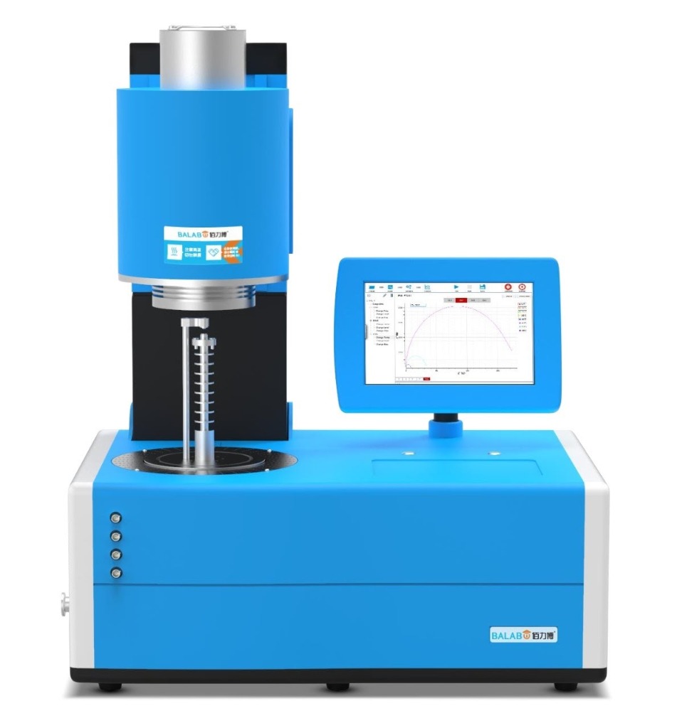
MatMeas DMS1000 High-Temperature Dielectric Spectrometer
The MatMeas DMS1000 is an advanced High-Temperature Dielectric Impedance Temperature Spectrometer engineered for the ultimate electrical characterization of bulk materials. Delivering an exceptional measurement accuracy of 0.05%, it operates efficiently from Room Temperature (RT) to 1000°C. Its upgraded platform supports both single-sample and four-sample simultaneous measurements. Integrated with a sealable metal shielding system and high-purity platinum electrodes, the DMS1000 enables highly reliable testing across inert, oxidizing, reducing, and vacuum atmospheres, making it an indispensable infrastructure for precision materials science.
View details →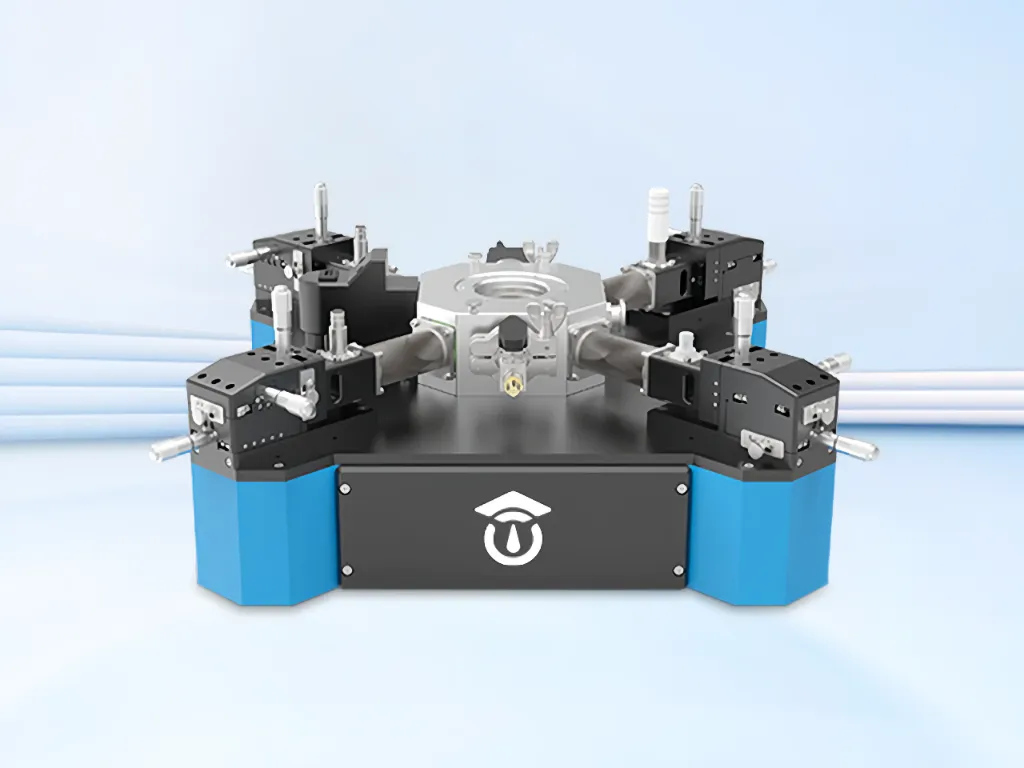
CPS7000 High-Low Temperature Dielectric Vacuum Probe Station
The MatMeas CPS7000 is an advanced, highly integrated desktop High-Low Temperature Dielectric Vacuum Probe Station engineered for the rigorous electrical characterization of thin films, bulk materials, and semiconductor wafers. Delivering performance directly comparable to industry-leading American brands like Lake Shore and Janis, this compact platform offers an ultra-wide temperature range from -160°C to 450°C via liquid nitrogen cooling. Uniquely equipped with a proprietary built-in air shock anti-vibration system, the CPS7000 eliminates data jumping points during continuous temperature variations. Supporting complex high-voltage and low-current testing environments, it is the ultimate infrastructure for evaluating dielectric, piezoelectric, ferroelectric, and TSDC properties in high-vacuum conditions.
View details →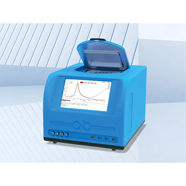
MatMeas DMS2000 High-Low Temperature Dielectric Spectrometer
The MatMeas DMS2000 is an advanced High and Low Temperature Dielectric Impedance Spectrometer engineered for evaluating the dielectric properties of materials under extreme thermal conditions. Compliant with the ASTM D150 standard, it integrates a proprietary LNP-95 liquid nitrogen injection system to achieve seamless continuous temperature variation from -160°C to 450°C. Uniquely featuring a vacuum-enabled sample chamber to completely prevent thermal frosting and eliminate false water peaks near 0°C, along with versatile options for single-sample or five-sample simultaneous testing, the DMS2000 ensures unparalleled data fidelity and high throughput for advanced scientific research.
View details →Request High-Precision Testing Solutions
Get expert guidance and customized instruments for your functional materials project.