Dielectric and Impedance Characterization of Ceramic Substrates: Brick-Layer Modeling and Spectrum Analysis
Technical News
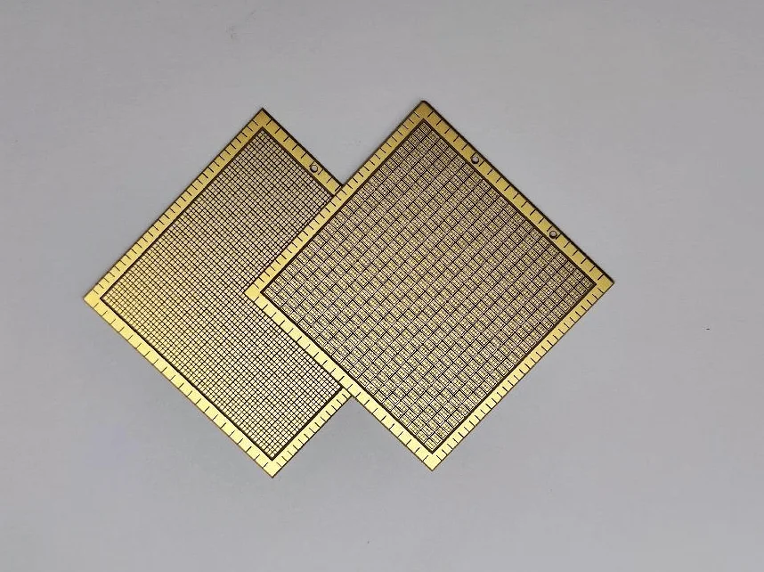
Advanced ceramic substrates—predominantly high-purity alumina (Al2O3), aluminum nitride (AlN), silicon nitride (Si3N4), and low-temperature co-fired ceramics (LTCC)—are the linchpins of modern high-voltage power electronics and high-frequency communication modules. In automotive traction inverters, wind turbine power stacks, photovoltaic converters, and 5G/6G millimeter-wave packaging, ceramic substrates must provide rigid mechanical support and superior thermal dissipation while maintaining near-perfect electrical isolation across broad temperature and frequency envelopes.
A fundamental shortcoming in traditional quality inspection is relying on single-frequency room-temperature capacitance and dissipation factor (tan delta) measurements (such as 1 kHz or 1 MHz at 25 C). Polycrystalline technical ceramics are heterogeneous microstructures consisting of semiconducting or insulating crystalline grains, highly disordered and defect-rich grain boundaries, secondary intergranular glassy phases, and metal-ceramic electrode contact interfaces. A single scalar value cannot reveal which microstructural feature is responsible for dielectric loss, localized leakage, or high-temperature degradation.
Electrochemical Impedance Spectroscopy (EIS) and Broadband Dielectric Spectroscopy (BDS)—governed by ASTM D150, IEC 60250, and SEMI G44—bridge the gap between microstructural physics and macroscopic electrical performance. By sweeping frequency across six to eight decades (from 10 uHz up to 30 MHz or 120 MHz) over temperatures spanning -160 C to +1000 C, impedance analysis deconvolves bulk grain conduction from grain boundary barriers and electrode polarization, providing actionable diagnostic insight for materials scientists and electronic packaging engineers.
The Brick-Layer Model and Equivalent Circuit Deconvolution
The standard theoretical framework for modeling electrical transport in polycrystalline electroceramics is the classical Brick-Layer Model. The ceramic microstructure is idealized as an array of cubic, conductive crystalline grains (representing the bulk material) separated by thin, contiguous, high-resistivity grain boundary layers.
When an alternating electric field traverses this heterogeneous microstructure, charges accumulate at the interfaces between regions of differing conductivities and permittivities (the Maxwell-Wagner-Sillars interfacial effect). Each distinct microstructural region behaves as a parallel combination of a resistor R (representing ohmic charge conduction) and a capacitor C (representing reversible dielectric polarization).
The total complex impedance Z*(omega) of the ceramic substrate is mathematically formulated as the series summation of these parallel R-C Voigt elements:
Z*(omega) = Z_bulk(omega) + Z_gb(omega) + Z_el(omega)
Z*(omega) = [R_g / (1 + j * omega * R_g * C_g)] + [R_gb / (1 + j * omega * R_gb * C_gb)] + [R_el / (1 + j * omega * R_el * C_el)]
Where:
- Z_bulk (R_g, C_g): The resistance and capacitance of the interior crystalline grains (bulk).
- Z_gb (R_gb, C_gb): The resistance and capacitance of the grain boundaries and intergranular amorphous glassy phases.
- Z_el (R_el, C_el): The resistance and capacitance associated with the metal electrode-ceramic contact interface (Schottky barrier, chemical interdiffusion, or double-layer charge accumulation).
- omega: The angular excitation frequency (omega = 2 * pi * f).
- j: The imaginary unit (j = sqrt(-1)).
Relaxation Time Constants and Semicircular Arc Deconvolution
On a complex impedance Nyquist plot (-Z'' versus Z'), each parallel R-C sub-circuit traces out a distinct semicircular arc whose diameter corresponds to the resistance R of that microstructural region, and whose summit satisfies the characteristic resonance condition:
omega_max * tau = omega_max * R * C = 2 * pi * f_max * R * C = 1
f_max = 1 / (2 * pi * R * C)
Because the capacitance C of each microstructural component differs by orders of magnitude based on its effective geometric thickness (C = epsilon_0 * epsilon_r * A / d_eff):
- Bulk Grain Interior (High Frequency): The grain interior occupies nearly the entire sample volume, resulting in an effective thickness equal to the macroscopic specimen thickness. Consequently, its capacitance C_g is small (typically 1 pF to 50 pF), placing its characteristic relaxation frequency f_max in the radio-frequency domain (f_max > 100 kHz to 30 MHz).
- Grain Boundaries (Intermediate Frequency): Grain boundaries represent ultra-thin intergranular layers (typically 1 nm to 10 nm in physical thickness). Because capacitance is inversely proportional to thickness, grain boundary capacitance C_gb is orders of magnitude larger (typically 1 nF to 100 nF), shifting its semicircular arc into the intermediate frequency band (100 Hz to 100 kHz).
- Electrode Interfaces (Low Frequency): Contact interfaces and blocking electrode double layers have effective thicknesses in the nanometer range, resulting in massive capacitances C_el (typically 1 uF to 100 uF). This produces an impedance arc or low-frequency spur at frequencies below 10 Hz.
Constant Phase Elements (CPE) for Depressed Arcs
In real polycrystalline ceramics, grain sizes are distributed log-normally, and grain boundaries possess varying tilt angles and tortuous geometries. Consequently, experimental Nyquist arcs are vertically depressed below the real axis. To model this non-Debye distributed relaxation, ideal capacitors are replaced with Constant Phase Elements (CPE):
Z_CPE(omega) = 1 / [Q_0 * (j * omega)^n]
Where Q_0 is a pseudo-capacitance parameter, and the exponent n (0 < n <= 1) quantifies the degree of microstructural inhomogeneity. When n = 1, the CPE behaves as an ideal capacitor; when n < 1, the angle of depression of the Nyquist semicircle is given by (1 - n) * 90 degrees.
Microstructural Origin and Frequency Classification Matrix
The diagnostic criteria for attributing impedance arcs to specific physical features in ceramic substrates are summarized in the table below.
| Microstructural Zone | Characteristic Capacitance Range | Typical Frequency Regime (at 300 C) | Nyquist Semicircle Feature | Physical / Chemical Mechanism | Influence on Electronic Packaging Performance |
|---|---|---|---|---|---|
| Bulk Grain Interior | 1 pF to 50 pF (per cm2) | High frequency (100 kHz to 30 MHz+) | High-frequency arc intercepting origin at Z' = 0 | Intrinsic crystal lattice ionic and electronic displacement | Determines high-frequency signal propagation delay and intrinsic dielectric loss |
| Grain Boundary Core | 1 nF to 50 nF (per cm2) | Intermediate frequency (100 Hz to 100 kHz) | Central dominant semicircle | Oxygen vacancy segregation, space-charge depletion barriers | Dictates bulk electrical breakdown strength and DC insulation leakage resistance |
| Intergranular Glass Phase | 100 pF to 5 nF (per cm2) | Intermediate to high frequency | Asymmetric shoulder on grain boundary arc | Silicate sintering aid glassy wetting layers | Can soften at high temperatures, creating parasitic high-temperature loss spikes |
| Electrode Contact Barrier | 1 uF to 50 uF (per cm2) | Low to ultra-low frequency (< 0.1 Hz to 100 Hz) | Low-frequency giant arc or steep capacitive tail | Schottky depletion layer, redox reactions, ion blocking | Influences contact resistance, interfacial delamination, and partial discharge ignition |
Immittance Formalisms: Decoupling Bulk Conduction via Combined Plots
In highly conductive or high-temperature ceramics, the low-frequency grain boundary and electrode arcs become so massive that they completely compress and obscure the minute bulk grain semicircle on standard Nyquist plots.
To overcome this, researchers simultaneously analyze four interrelated immittance formalisms:
- Complex Impedance: Z*(omega) = Z' - j * Z'' = R + j * X (highlights high-resistance components).
- Complex Admittance: Y*(omega) = 1 / Z* = Y' + j * Y'' = G + j * B (highlights low-resistance, high-conductance paths).
- Complex Electric Modulus: M*(omega) = j * omega * C_0 * Z* = M' + j * M'' = 1 / epsilon* (suppresses electrode polarization and highlights bulk dielectric relaxations).
- Complex Permittivity: epsilon*(omega) = 1 / M* = epsilon' - j * epsilon'' (highlights capacitive energy storage and dissipation).
By plotting normalized imaginary impedance (Z'' / Z''_max) and normalized imaginary modulus (M'' / M''_max) against logarithmic frequency on a single shared Bode graph, researchers can immediately determine whether localized or long-range conduction dominates:
- If the Z'' and M'' peak frequencies coincide collinearly (f_max,Z = f_max,M), the relaxation is governed by localized, long-range carrier hopping through an idealized single-time-constant network.
- If the Z'' and M'' peaks are separated by several decades of frequency (f_max,M >> f_max,Z), the material contains multiple heterogeneous phases, where M'' isolates the bulk grain relaxation and Z'' reflects grain boundary and electrode barrier impedance.
Material Benchmark Comparison: Dielectric and Impedance Parameters Across Substrates
The following benchmark table provides experimentally extracted bulk grain resistances, grain boundary activation energies, and dielectric properties across commercial electronic ceramic substrates.
| Ceramic Substrate Formulation | Sintering Aids / Grain Morphology | Bulk Resistance R_g at 400 C (kOhm*cm) | Grain Boundary R_gb at 400 C (kOhm*cm) | Grain Boundary Activation Energy E_a (eV) | Permittivity epsilon_r' (1 MHz, 25 C) | Loss Tangent tan delta (1 MHz, 25 C) | Dominant Conduction Carrier |
|---|---|---|---|---|---|---|---|
| Alumina 96% (Al2O3) | 4% SiO2-CaO-MgO liquid phase | 150 to 300 | 1,200 to 2,500 | 1.15 to 1.30 | 9.4 | 0.0010 | Doubly ionized oxygen vacancies + alkali impurity ions |
| High-Purity Alumina 99.6% | 0.4% MgO (solid-state sintered) | 800 to 1,500 | 15,000 to 35,000 | 1.45 to 1.65 | 9.9 | 0.0002 | Pure intrinsic oxygen vacancy hopping |
| Aluminum Nitride (AlN) | 3% Y2O3 (yttrium aluminate GB) | 50 to 120 | 800 to 1,800 | 1.05 to 1.25 | 8.9 | 0.0006 | Aluminum vacancies and oxygen-on-nitrogen defect complexes |
| Silicon Nitride (Si3N4) | Al2O3-Y2O3 intergranular phase | 80 to 200 | 1,500 to 3,200 | 1.20 to 1.40 | 8.1 | 0.0025 | Intergranular glassy phase ionic hopping |
| LTCC Glass-Ceramic | Crystallized anorthite/celsian glass | 10 to 40 | 150 to 450 | 0.85 to 1.05 | 6.2 | 0.0020 | Modifying alkali and alkaline-earth mobile cations |
| Barium Titanate Dielectric | Core-shell BaTiO3 grains | 0.5 to 2.0 | 50 to 200 | 0.75 to 0.90 | 2500 to 3500 | 0.0150 | Grain boundary re-oxidized space-charge barrier |
Hardware Instrumentation Platforms: MatMeas DMS-1000, DMS-2000, and CPS-7000
Acquiring pristine, reproducible impedance spectra across wide temperature and frequency spans requires hardware engineered to eliminate thermal lag, electromagnetic cross-talk, and environmental artifacts.
The flagship MatMeas DMS-1000 High-Temperature Dielectric Spectrometer provides an industry-leading platform for bulk ceramic substrates and refractory solids. Operating from 20 Hz to 30 MHz (expandable to 120 MHz) up to +1000 C, the DMS-1000 incorporates an active metal shielding enclosure that blocks high-current AC heating coil interference. A coplanar thermocouple sensor positioned within 0.5 mm of the substrate face ensures real-time temperature tracking without thermal lag, delivering 0.05% basic impedance measurement accuracy.
For applications requiring characterization down to deep cryogenic temperatures—critical for satellite communications, superconducting power systems, and quantum computing packaging—the MatMeas DMS-2000 High-Low Temperature Dielectric Spectrometer spans an ultra-wide thermal range from -160 C up to +500 C. Utilizing an advanced liquid nitrogen injection vaporization system (LNP-95), the DMS-2000 maintains continuous temperature sweeps within +/-0.5 C stability without boiling vibration. Crucially, the DMS-2000 incorporates a high-vacuum sample chamber (< 10^-3 Pa) that eliminates atmospheric moisture condensation, preventing frost-induced parasitic capacitance spikes near 0 C.
When characterizing localized micro-regions, unpackaged thin-film patterns, or diced semiconductor dies, the MatMeas CPS-7000 High-Low Temperature Dielectric Vacuum Probe Station delivers high-resolution micro-probing. Featuring four independently adjustable triaxial probe arms and integrated pneumatic anti-vibration suspension, the CPS-7000 isolates sample stages from building rumblings, ensuring stable probe contact on 20 um pads across a -160 C to +450 C thermal range.
Standardized Step-by-Step SOP for Impedance Spectroscopy
To obtain publication-grade impedance spectra complying with ASTM D150 and IEC 60250, testing technicians should follow this structured testing SOP:
Step 1: Specimen Preparation and Electrode Application
- Machine ceramic substrate test specimens as flat, parallel discs (recommended diameter 15 mm to 20 mm, thickness 0.5 mm to 1.0 mm; parallelism within +/-0.005 mm).
- Clean specimens ultrasonically in acetone, rinse in isopropanol, and bake at 120 C for 1 hour to drive out adsorbed surface moisture.
- Apply circular electrodes to opposing faces to form a parallel-plate geometry. Sputter 100 nm of platinum with a 10 nm titanium adhesion layer, or apply high-temperature platinum paste fired at 950 C. Maintain an unmetallized perimeter margin of at least 1.0 mm to prevent edge arcing.
Step 2: Fixture Calibration (Open-Short Compensation)
- Mount the fixture inside the test chamber without the specimen. Execute an Open Circuit calibration across the full frequency band (20 Hz to 30 MHz) to compensate for fixture stray capacitance and leakage conductance.
- Short the upper and lower electrode contacts directly together. Execute a Short Circuit calibration to nullify fixture lead resistance and parasitic lead inductance.
Step 3: Specimen Installation and Contact Verification
- Install the metallized ceramic substrate centrally between the spring-loaded platinum contacts. Apply a uniform mechanical contact force (typically 1 N to 2 N).
- Measure the room-temperature complex impedance spectrum at an AC oscillation voltage of 100 mV RMS. Confirm that the measured series resistance and capacitance are stable and free from contact chatter.
Step 4: Temperature Sweeps and Spectrum Acquisition
- Program the temperature controller with defined thermal plateaus (e.g., from 100 C to 800 C in 50 C steps, at a ramp rate of 3 C/min to 5 C/min).
- At each temperature setpoint, enforce an isothermal dwell period of 5 minutes to ensure thermal equilibrium throughout the substrate thickness.
- Execute automated logarithmic frequency sweeps across the selected band (e.g., 50 points per decade from 20 Hz to 30 MHz).
- Export raw real impedance Z', imaginary impedance Z'', phase angle theta, and frequency f data into equivalent circuit fitting software (such as ZView or equivalent non-linear least-squares fitting algorithms).
Frequently Asked Questions (FAQ)
How does complex impedance spectroscopy distinguish bulk grains from grain boundaries in ceramic substrates?
Because of their microscopic geometry, bulk grains and grain boundaries have vastly different effective capacitances. Bulk grains have capacitances in the picofarad (pF) range, while nanometer-thick grain boundaries have capacitances in the nanofarad (nF) range. Because the relaxation frequency is inversely proportional to capacitance (f_max = 1 / (2 * pi * R * C)), bulk grains relax at high frequencies (> 100 kHz), while grain boundaries relax at intermediate frequencies (< 10 kHz), appearing as separate, deconvolutable semicircular arcs on a Nyquist plot.
Why is an active guard shielding system necessary in high-temperature impedance furnaces?
Electric furnaces rely on high-power resistive heating coils that switch large alternating currents. Without electrostatic shielding, electromagnetic radiation from these coils couples directly into the high-impedance measurement leads, creating massive 50 Hz/60 Hz harmonic spikes that distort impedance data. The DMS-1000 incorporates an internal grounded metal shield and coaxial lead routing that completely isolates the sample from furnace noise.
What is the purpose of Open-Short-Load (OSL) calibration in broadband testing?
At frequencies above 1 MHz, the physical inductance of high-temperature metallic extension leads and the stray capacitance between fixture terminals become comparable to the impedance of the specimen under test. Without calibration, lead inductance causes false resonant peaks that artificially inflate capacitance. Open-Short calibration shifts the measurement reference plane directly to the sample faces, eliminating fixture parasitics.
Why does atmospheric moisture condensation ruin cryogenic dielectric measurements near 0 C?
When unsealed fixtures are cooled below ambient temperature using liquid nitrogen, atmospheric humidity freezes onto the sample surface, forming ice crystals. Near 0 C, the ice melts and undergoes intense dipolar relaxation, producing a massive false dielectric loss peak (often called a "water peak") that completely masks the material's genuine cryogenic properties. Operating in high vacuum (< 10^-3 Pa), as provided by the DMS-2000, ensures a 100% frost-free environment.
Related Instruments & Equipment
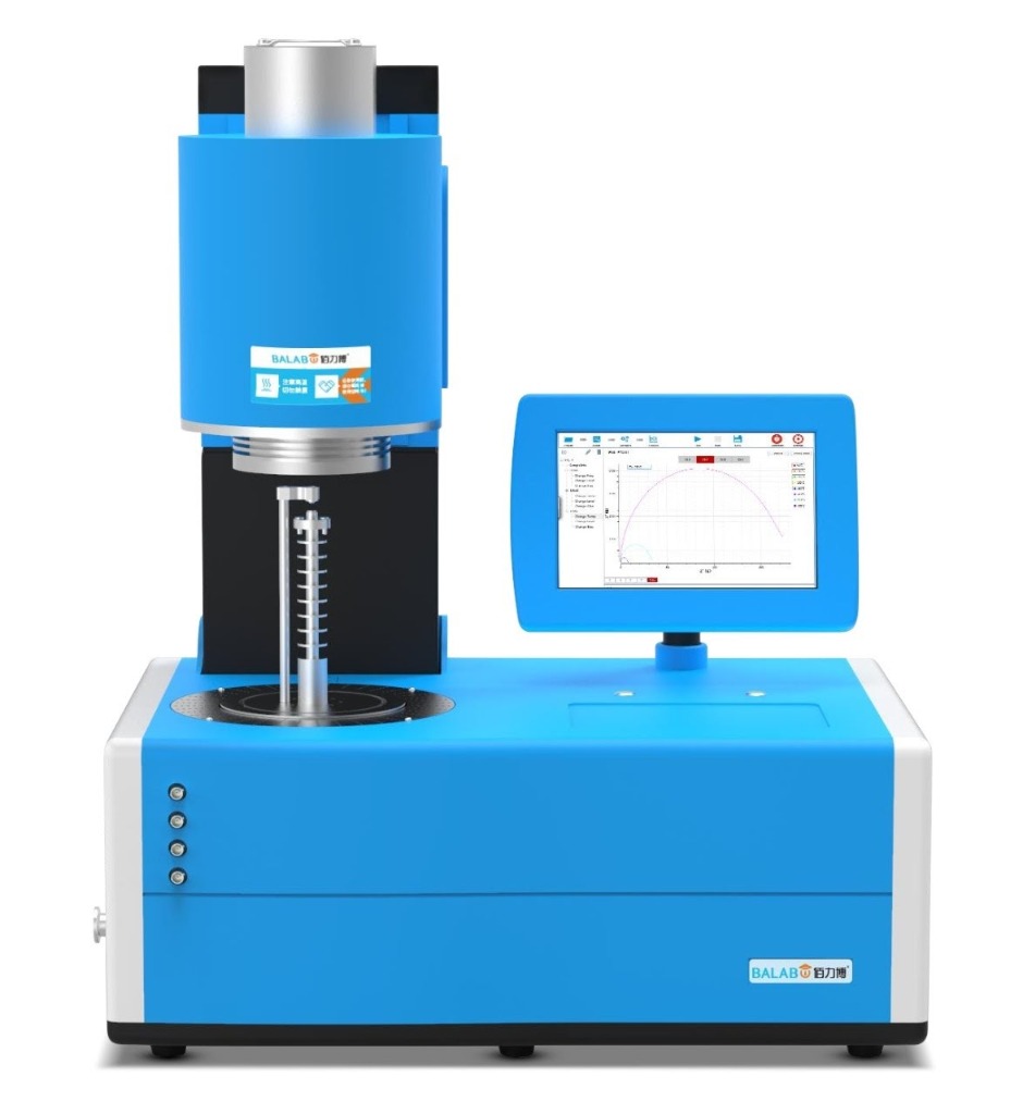
MatMeas DMS1000 High-Temperature Dielectric Spectrometer
The MatMeas DMS1000 is an advanced High-Temperature Dielectric Impedance Temperature Spectrometer engineered for the ultimate electrical characterization of bulk materials. Delivering an exceptional measurement accuracy of 0.05%, it operates efficiently from Room Temperature (RT) to 1000°C. Its upgraded platform supports both single-sample and four-sample simultaneous measurements. Integrated with a sealable metal shielding system and high-purity platinum electrodes, the DMS1000 enables highly reliable testing across inert, oxidizing, reducing, and vacuum atmospheres, making it an indispensable infrastructure for precision materials science.
View details →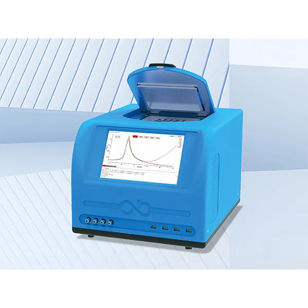
MatMeas DMS2000 High-Low Temperature Dielectric Spectrometer
The MatMeas DMS2000 is an advanced High and Low Temperature Dielectric Impedance Spectrometer engineered for evaluating the dielectric properties of materials under extreme thermal conditions. Compliant with the ASTM D150 standard, it integrates a proprietary LNP-95 liquid nitrogen injection system to achieve seamless continuous temperature variation from -160°C to 450°C. Uniquely featuring a vacuum-enabled sample chamber to completely prevent thermal frosting and eliminate false water peaks near 0°C, along with versatile options for single-sample or five-sample simultaneous testing, the DMS2000 ensures unparalleled data fidelity and high throughput for advanced scientific research.
View details →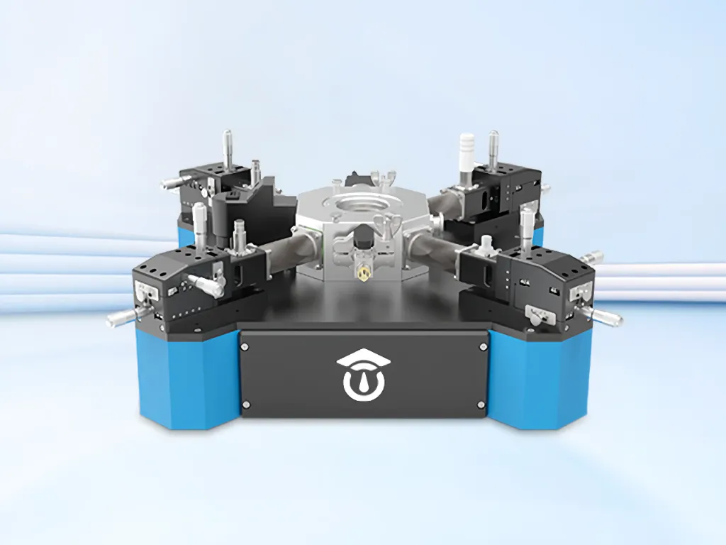
CPS7000 High-Low Temperature Dielectric Vacuum Probe Station
The MatMeas CPS7000 is an advanced, highly integrated desktop High-Low Temperature Dielectric Vacuum Probe Station engineered for the rigorous electrical characterization of thin films, bulk materials, and semiconductor wafers. Delivering performance directly comparable to industry-leading American brands like Lake Shore and Janis, this compact platform offers an ultra-wide temperature range from -160°C to 450°C via liquid nitrogen cooling. Uniquely equipped with a proprietary built-in air shock anti-vibration system, the CPS7000 eliminates data jumping points during continuous temperature variations. Supporting complex high-voltage and low-current testing environments, it is the ultimate infrastructure for evaluating dielectric, piezoelectric, ferroelectric, and TSDC properties in high-vacuum conditions.
View details →Request High-Precision Testing Solutions
Get expert guidance and customized instruments for your functional materials project.