Cyclic-Force Open-Circuit Voltage Testing of Piezoelectric Films
Technical News
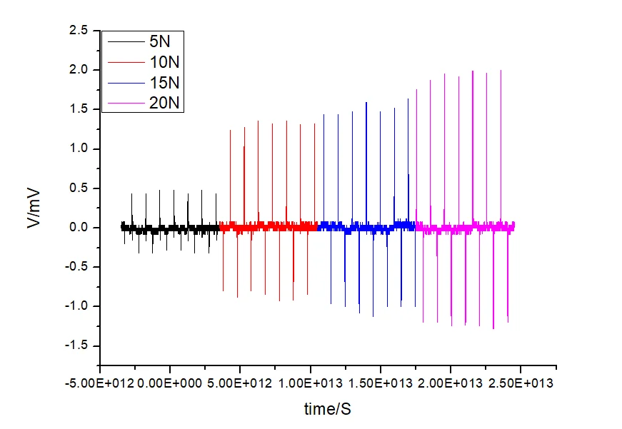
Piezoelectric thin and thick films—including aluminum nitride (AlN), scandium-doped aluminum nitride (AlScN), lead zirconate titanate (PZT), barium titanate (BaTiO3), and poly(vinylidene fluoride) polymers (PVDF and P(VDF-TrFE))—serve as the transduction engines for piezoelectric micromachined ultrasonic transducers (PMUTs), vibration energy harvesters (PEHs), MEMS acoustic sensors, and flexible epidermal monitors. In these dynamic operating architectures, the transducer converts mechanical strain or alternating surface stress into transient electrical signals across millions, or even billions, of mechanical cycles.
Measuring the open-circuit voltage (V_oc) generated under cyclic uniaxial or flexural force loading provides an essential figure of merit for sensor sensitivity and energy harvesting potential. However, a widespread metrological misconception treats open-circuit voltage as an intrinsic scalar material constant. In physical reality, V_oc is an extrinsic system-level response that depends strongly on sample capacitance, cable parasitics, electrometer input impedance, excitation frequency, mechanical prestress, and substrate elastic clamping.
Furthermore, subjecting films to sustained alternating stresses triggers mechanical, electrical, and interfacial fatigue. Domain wall pinning, micro-crack propagation in brittle oxide films, metal electrode delamination, and local depoling degrade output voltage over time. Establishing a rigorous testing protocol requires understanding the coupled electromechanical constitutive laws, instrument boundary conditions, and degradation kinetics.
Electromechanical Constitutive Equations and Open-Circuit Voltage Theory
Under one-dimensional compressive stress applied along the polar thickness axis (direction 3), the direct piezoelectric effect is governed by the linear constitutive equations defined in IEEE Std 176 and IEC 60483:
D3 = d33 * T3 + epsilon33_T * E3
S3 = s33_E * T3 + d33 * E3
Where D3 is the electric displacement, T3 is the mechanical stress, epsilon33_T is the stress-free dielectric permittivity, E3 is the internal electric field, S3 is mechanical strain, and s33_E is the elastic compliance at zero electric field.
+---------------------------------------------------------------------------------------------------+
|                        Piezoelectric Film Uniaxial Compression Dynamics                           |
+---------------------------------------------------------------------------------------------------+
|                                                                                                   |
|           F_dynamic(t) = F_static + delta_F * sin(omega * t)  [Actuator Load]                      |
|                               |                                                                   |
|                               v                                                                   |
|            +------------------------------------+  Top Electrode (Area A)                         |
|            |  P_s  |  P_s  |  P_s  |  P_s  |  P_s |                                               |
|            |  |||  |  |||  |  |||  |  |||  |  ||| |  Piezoelectric Active Film (Thickness h)      |
|            |  vvv  |  vvv  |  vvv  |  vvv  |  vvv |                                               |
|            +------------------------------------+  Bottom Electrode / Substrate                   |
|                                                                                                   |
|            Open-Circuit Condition (D3 = 0)  ===>  Generated Field: E3 = - (d33 / epsilon33_T) * T3|
+---------------------------------------------------------------------------------------------------+
In a true open-circuit condition, zero net current flows through the external circuit, constraining the electric displacement to zero (D3 = 0). Substituting this boundary condition into the constitutive relation yields the internal electric field generated across the film thickness:
E3 = - (d33 / epsilon33_T) * T3 = - g33 * T3
Where g33 is the longitudinal piezoelectric voltage coefficient:
g33 = d33 / (epsilon_0 * epsilon_r)
The theoretical peak-to-peak open-circuit voltage (V_oc) developed across a film of thickness h and active electrode area A under an alternating dynamic force delta_F (stress T3 = delta_F / A) is given by:
V_oc = integral_0^h E3 dz = g33 * (delta_F / A) * h = (d33 / (epsilon_0 * epsilon_r)) * (delta_F / A) * h
Recognizing that the intrinsic sample capacitance (C_sample) is:
C_sample = (epsilon_0 * epsilon_r * A) / h
The open-circuit voltage equation reduces to the fundamental electrostatic charge-capacitance balance:
V_oc = Q_piezo / C_sample = (d33 * delta_F) / C_sample
This formulation exposes a critical engineering trade-off: while increasing film thickness h or reducing relative permittivity epsilon_r boosts the generated voltage, it simultaneously diminishes sample capacitance and available charge, dictating the optimal power transfer impedance.
The Electrical Boundary Condition: Finite Input Impedance and Parasitic Attenuation
In a physical laboratory environment, an ideal open-circuit condition (infinite load resistance and zero stray capacitance) cannot be achieved. The test specimen is connected via coaxial cables to an oscilloscope, lock-in amplifier, or high-impedance electrometer. The equivalent measurement circuit comprises the piezoelectric charge generator in parallel with the intrinsic sample capacitance (C_sample), cable capacitance (C_cable), instrument input capacitance (C_in), and instrument input resistance (R_in).
   Piezoelectric Film Equivalent Circuit Connected to Measurement Front-End:

       +---------------+-----------+-----------+-----------+
       |               |           |           |           |
       O               |           |           |           |
      (~) Q(t)        --- C_sample--- C_cable --- C_in    [R_in]
     Generator        ---         ---         ---          |
       |               |           |           |           |
       +---------------+-----------+-----------+-----------+
       |                                                   |
      GND                                                 GND
This electrical network introduces two severe distortion mechanisms:
1. Capacitive Voltage Attenuation
The total effective capacitance (C_total) loading the piezoelectric charge generator is:
C_total = C_sample + C_cable + C_in
Because the total piezoelectric charge Q_piezo is distributed across all parallel capacitive branches, the actual observable voltage (V_measured) is severely attenuated:
V_measured = V_oc * [C_sample / (C_sample + C_cable + C_in)]
For a typical MEMS piezoelectric thin film (thickness h = 1 um, area A = 1 mm2, epsilon_r = 15 for AlN), the intrinsic capacitance is:
C_sample = (8.854e-12 * 15 * 1e-6) / 1e-6 = 0.133 nF (133 pF)
A standard 1-meter RG-58 coaxial cable introduces approximately 100 pF of stray capacitance, and a standard oscilloscope introduces 15 pF in parallel with 1 megaohm. The measured voltage will be:
V_measured = V_oc * [133 / (133 + 100 + 15)] = 0.536 * V_oc
Nearly 46% of the true open-circuit voltage is lost to cable parasitics. To measure true V_oc, active high-impedance buffer preamplifiers (input capacitance < 1 pF, input resistance > 1e12 ohms) must be placed directly adjacent to the contact probe tips.
2. Low-Frequency High-Pass Filtering and RC Charge Drainage
The parallel combination of total capacitance (C_total) and instrument input resistance (R_in) forms a high-pass filter with a characteristic RC discharge time constant (tau):
tau = R_in * C_total
The lower cut-off frequency (f_cutoff, -3 dB point) below which the generated charge drains before peak voltage can be detected is:
f_cutoff = 1 / (2 * pi * tau) = 1 / (2 * pi * R_in * C_total)
If the mechanical cyclic excitation frequency (f_exc) is lower than 3 * f_cutoff, the output waveform is severely differentiated: sinusoidal force excitation produces an asymmetrical distorted waveform with significant phase advance and attenuated peak voltage. Ensuring a measurement error below 1% requires:
tau >= 10 / (2 * pi * f_exc) ===> R_in >= 10 / (2 * pi * f_exc * C_total)
For low-frequency biomechanical or human-motion testing (f_exc = 1 Hz) on small-capacitance films (C_total = 200 pF), the instrument input resistance must satisfy R_in >= 8e10 ohms (80 gigaohms), rendering standard 1-megaohm or 10-megaohm oscilloscope inputs useless.
Operating Modes Comparison Matrix: Open-Circuit vs Short-Circuit vs Load
The table below outlines the three fundamental electrical boundary conditions utilized when characterizing piezoelectric film dynamic electromechanical responses.
| Metrological Parameter | Open-Circuit Voltage Mode (V_oc) | Short-Circuit Charge Mode (Q_sc) | Impedance-Matched Load Mode (P_max) |
|---|---|---|---|
| Circuit Boundary | High-impedance buffer (R_in > 1e12 ohms) | Virtual-ground transimpedance amplifier (TIA) | Resistive load matching source impedance (R_L = R_opt) |
| Primary Output Metric | Voltage sensitivity g33, internal electric field | Transferred charge Q, dynamic strain d33 | Continuous delivered electrical power P_out, energy density |
| Capacitance Sensitivity | High; attenuated by C_cable and C_in | Zero; virtual ground holds V = 0, shunting stray capacitance | High; peak power depends strictly on source reactance |
| Frequency Dependence | Differentiates signal if f_exc < 1 / (2 * pi * tau) | Flat broadband frequency response from DC to 100 kHz | Shifts optimal load resistance: R_opt = 1 / (omega * C_sample) |
| Piezoelectric Figure of Merit | Voltage factor: g33 = d33 / (epsilon_0 * epsilon_r) | Charge factor: d33 = Q / F | Power factor: (d33^2) / (epsilon_0 * epsilon_r) |
| Primary Failure Artifact | Charge leakage across cable insulation resistance | Op-amp input offset current and saturation drift | Non-linear resistive heating in thin-film contacts |
| Applicable Standards | IEEE Std 176, SEMI MS4-0307 | IEC 60483, ASTM D150 | ASTM F668, IEEE Std 180 |
Mechanical Cyclic Fatigue and Degradation Mechanisms
When thin films are subjected to high-cycle alternating stress (1e6 to 1e9 cycles), the generated open-circuit voltage and piezoelectric charge decay over time. In ferroelectric and piezoelectric thin films, fatigue arises from coupled mechanical, microstructural, and electrical phenomena:
+---------------------------------------------------------------------------------------------------+
|                        Thin-Film Mechanical Cyclic Fatigue Mechanisms                             |
+---------------------------------------------------------------------------------------------------+
|  [Mechanism A: 90-Degree Domain Wall Pinning]                                                     |
|  Cyclic shear stress drives oxygen vacancies toward domain boundaries -> locks domain mobility.   |
|                                                                                                   |
|  [Mechanism B: Interfacial Delamination & Micro-Cracking]                                         |
|  Elastic modulus mismatch between film and substrate generates interface shear cracks -> open     |
|  circuits.                                                                                        |
|                                                                                                   |
|  [Mechanism C: Metal Electrode Fatigue & Micro-Fretting]                                          |
|  Cyclic contact pressure induces fretting wear, micro-cracking, and localized resistance rise.    |
+---------------------------------------------------------------------------------------------------+
The decay in effective piezoelectric response d33(N) as a function of cycle count N frequently follows a logarithmic degradation model:
d33(N) = d33_0 * [1 - k_fatigue * log10(N / N_0)]
Where d33_0 is the baseline response at cycle N_0, and k_fatigue is the mechanical fatigue degradation rate. In ferroelectric perovskite films like PZT, k_fatigue is strongly dependent on the alternating stress amplitude (delta_T) and the static preload clamping stress (T_static).
The table below summarizes common fatigue mechanisms and their engineering mitigation protocols.
| Degradation Mechanism | Physical Root Cause | Observed Electrical Signature | Diagnostic Verification & Mitigation Protocol |
|---|---|---|---|
| Domain Pinning by Point Defects | Oxygen vacancy migration and agglomeration at 90-degree domain walls | Gradual drop in V_oc and d33; increase in mechanical quality factor Q_m | Apply unipolar high-voltage refreshing pulses to de-pin domain walls |
| Top Electrode Micro-Fretting | Cyclic abrasive wear between mechanical contact tip and thin gold electrode | Voltage waveform becomes noisy; contact resistance increases | Utilize spherical sapphire contact tips coated with conductive elastomer |
| Substrate Interfacial Delamination | Shear stress concentration at film-substrate interface due to CTE/stiffness mismatch | Abrupt catastrophic drop in V_oc; erratic capacitance fluctuations | Introduce thin metallic adhesion interlayers (Ti, Cr); verify via SEM |
| Micro-Crack Propagation | Tensile stress exceedance in brittle ceramic film during flexural cycling | Step-like decreases in capacitance; permanent drop in dielectric breakdown field | Optimize neutral mechanical axis positioning in flexural cantilever stacks |
| Thermal Depoling via Self-Heating | Mechanical internal friction (tan delta_m) converts cyclic energy to heat | Monotonic downward drift in V_oc; baseline DC pyroelectric drift | Monitor in-situ sample temperature; operate below critical heat flux |
Instrumentation Architecture: Dynamic In-Situ Testing Platforms
Characterizing thin-film cyclic voltage response demands specialized mechanical loading platforms capable of applying millinewton-level dynamic forces while maintaining rigid coaxial alignment. Traditional Berlincourt meters utilize coarse spring clamps and manual screw mechanisms that apply uncalibrated preloads (often 2 N to 10 N), fracturing fragile sub-micron films or inducing severe mechanical depoling.
The MatMeas PEAI-1000 High-Precision Piezoelectric Analyzer provides independent closed-loop control of static clamping preload (1.0 N to 10.0 N) and dynamic cyclic force (0.05 N to 0.5 N). Featuring built-in lock-in amplification, it isolates weak micro-volt piezoelectric signals from ambient industrial 50/60 Hz electromagnetic pickup, providing ultra-low-noise voltage sensitivity measurements.
For long-duration mechanical endurance studies requiring continuous frequency sweeps and high cycle accumulation (up to 1e7 cycles), the MatMeas PEMS-1000 In-Situ Dynamic Piezoelectric System incorporates an electrodynamic shaker with automated load-cell feedback. Its servo-driven stage compensates dynamically for thermal expansion and fixture mechanical relaxation, maintaining a constant force amplitude across extended fatigue tests from 30 Hz to 300 Hz.
Best-Practice Laboratory SOP for Thin-Film Cyclic Voltage and Fatigue Testing
To achieve reproducible, peer-reviewed cyclic voltage data, execute the following standardized procedure:
- Specimen Mounting and Contact Integrity:
- Mount the thin-film chip onto a rigid, polished anvil to eliminate parasitic bending modes unless flexural bending is intentionally tested.
- Verify that the bottom ground electrode provides a low-resistance ohmic contact (< 1 ohm) across the entire substrate backplane.
- Pre-Test Baseline Metrology:
- Measure low-field capacitance (C_sample) and dielectric loss (tan delta) at 1 kHz using an impedance analyzer.
- Perform initial small-signal quasi-static d33 verification to record the baseline un-fatigued state.
- Fixture Alignment and Static Preload Setup:
- Align the upper loading probe coaxially with the center of the film top electrode.
- Apply a calibrated static preload force (F_static, typically 0.5 N to 1.0 N for thin films) to establish intimate mechanical contact and prevent the tip from bouncing or chattering during cyclic loading.
- Dynamic Force Calibration:
- Excite the electrodynamic shaker at the target frequency (e.g., 100 Hz) with a sinusoidal dynamic force amplitude (delta_F = 0.2 N RMS).
- Verify the force waveform using an in-line quartz dynamic load cell positioned directly above the specimen. Ensure total harmonic distortion (THD) of the mechanical force remains below 2%.
- High-Impedance Voltage Acquisition:
- Route the top electrode signal through an active electrometer buffer (input impedance > 100 gigaohms, input capacitance < 2 pF).
- Connect the buffer output to a digital storage oscilloscope or lock-in amplifier referenced to the shaker drive frequency.
- Continuous Cycling and Intermittent Interrogation:
- Log peak-to-peak open-circuit voltage (V_oc_pp), force amplitude, and electromechanical phase lag (theta) logarithmically (e.g., at 10^0, 10^1, 10^2, ..., 10^7 cycles).
Dynamic Stress Non-Linearity and the Mechanical Rayleigh Law in Thin Films
When piezoelectric thin films are subjected to variable-amplitude cyclic forces, their electromechanical response deviates from strict linear elasticity. In ferroelectric films such as sol-gel or sputtered PZT, domain walls interact with localized point defect pinning centers (such as oxygen vacancies and acceptor-dopant dipoles). Under cyclic dynamic stress amplitudes exceeding a threshold stress (T_th), irreversible domain wall unpinning occurs, producing a stress-dependent piezoelectric coefficient described by the mechanical Rayleigh law:
d33(delta_T) = d33_init + alpha_R * delta_T
Where:
- d33_init: The zero-field reversible piezoelectric coefficient, representing pure lattice distortion and reversible, elastic domain wall oscillations within shallow potential energy wells.
- alpha_R: The mechanical Rayleigh parameter, which quantifies the density of mobile ferroelectric domain walls and their propensity to overcome pinning obstacles under cyclic mechanical drive.
- delta_T: The alternating dynamic stress amplitude (delta_F / A).
Because open-circuit voltage scales with the dynamic charge output, the observed V_oc under large cyclic forces exhibits non-linear expansion:
V_oc(delta_T) = [(d33_init + alpha_R * delta_T) * delta_T * h] / (epsilon_0 * epsilon_r)
In energy harvesting and dynamic sensor applications, operating within the non-linear Rayleigh regime increases initial voltage generation but accelerates mechanical fatigue degradation. Irreversible domain wall motion generates internal mechanical friction, dissipating mechanical energy as heat:
W_loss = (4 / 3) * alpha_R * (delta_T)^3
Tracking the evolution of alpha_R across millions of cycles provides a sensitive, non-destructive probe of domain wall immobilization and defect clustering long before macro-cracking or electrode delamination manifests.
Frequently Asked Questions (FAQ)
Why does the open-circuit voltage change when switching between different test cables?
Coaxial cables introduce parasitic capacitance between the central conductor and the outer grounded shield, typically 60 to 100 pF per meter. Because a thin-film specimen possesses a finite intrinsic capacitance (C_sample), connecting a longer or higher-capacitance cable forms a capacitive voltage divider: V_meas = V_oc * [C_sample / (C_sample + C_cable)]. If a film has a capacitance of 100 pF and is measured with a 2-meter cable possessing 200 pF of capacitance, two-thirds of the generated voltage drops across the cable, causing a 67% underestimation. Always record and report total fixture and cable capacitance when publishing V_oc data.
Can open-circuit voltage alone determine the energy-harvesting capability of a piezoelectric film?
No. Open-circuit voltage represents the unloaded potential difference across the transducer, during which zero current is delivered to an external load (delivered power P = V * I = 0). Conversely, under short-circuit conditions, current is maximized while voltage drops to zero (P = 0). Usable energy harvesting occurs only when connected to a matched resistive-capacitive load:
R_opt = 1 / (omega * C_sample)
The maximum achievable average power (P_max) delivered to a matched load is:
P_max = (1 / 8) * omega * C_sample * V_oc_peak^2
A material exhibiting high V_oc but extremely low capacitance (such as an ultra-thin low-permittivity polymer) may generate substantial voltage spikes but deliver negligible energy compared to a lower-voltage, high-capacitance oxide film.
How does mechanical prestress influence the cyclic fatigue life of piezoelectric films?
A static mechanical compressive preload serves two opposing roles:
- Positive Contact Stabilization: It prevents mechanical tip chattering and ensures intimate stress transfer without impact hammering.
- Negative Ferroelastic Depoling: If the static compressive stress exceeds the mechanical coercive stress of the material (typically 10 to 50 MPa for PZT), it drives 90-degree domain wall switching into the orthogonal plane, mechanically depoling the film before fatigue cycling begins. For fragile oxide films, the static preload stress must be maintained below 10% of the film fracture strength, while ensuring that the dynamic force amplitude never unloads the tip into tensile separation.
Related Instruments & Equipment
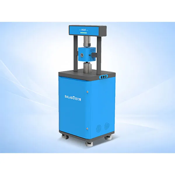
MatMeas High Precision In‑situ d33 Piezoelectric Measurement System – PEMS Analyzer
MatMeas PEMS is a high‑precision in‑situ d33 piezoelectric measurement system for advanced material characterization.
View details →
MatMeas PEAI1000 High-Precision Piezoelectric Analyzer
The MatMeas PEAI1000 is a next-generation High-Precision Piezoelectric Analyzer engineered to evaluate the piezoelectric coefficient (d33) of advanced functional materials. Surpassing the limitations of traditional d33 measuring instruments, it employs an advanced dynamic measurement method integrated with cutting-edge lock-in amplification technology. This architecture strictly suppresses environmental noise, significantly improving the signal-to-noise ratio. Capable of applying variable static clamping forces (1~10N) and precise dynamic test forces (0.1~0.5N), it guarantees an ultra-wide measurement range (0 to 2000 pC/N) with an exceptional accuracy of ±2%. It is an essential, highly reliable tool for the research, application, and mass production of piezoelectric blocks, plates, and delicate thin films.
View details →Request High-Precision Testing Solutions
Get expert guidance and customized instruments for your functional materials project.