P-E Hysteresis Loop Testing of Ferroelectric Thin Films
Technical News
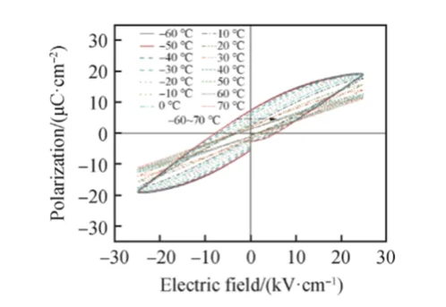
Ferroelectric thin films—including lead zirconate titanate (PZT), bismuth ferrite (BiFeO3), strontium bismuth tantalate (SBT), and emerging CMOS-compatible fluorite-structure oxides such as silicon- or zirconium-doped hafnium oxide (HfO2, HZO)—represent the physical foundation for non-volatile ferroelectric random-access memories (FeRAM), ferroelectric field-effect transistors (FeFETs), negative capacitance logic gates, and integrated electro-optic modulators. In these nanoscale thin-film devices, the definitive physical signature of ferroelectricity is the electric polarization versus electric field (P-E) hysteresis loop, which quantifies the spontaneous, field-reversible electric dipole moment per unit volume.
From a measured P-E loop, engineers extract core figures of merit: remanent polarization (P_r), saturation polarization (P_s), and positive and negative coercive fields (E_c+ and E_c-). In sub-micron and nanoscale thin films, however, extracting true ferroelectric parameters is notoriously vulnerable to severe experimental artifacts. Because dielectric thickness is on the order of 10 nm to 500 nm, operating electric fields exceed several megavolts per centimeter (MV/cm). Under these intense fields, non-ohmic conduction mechanisms (such as Fowler-Nordheim tunneling, Poole-Frenkel emission, and Schottky barrier leakage) generate large conductive currents that standard charge-integrating circuits misinterpret as massive polarization.
This artifact produces artificially inflated, rounded, or cigar-shaped loops—often referred to in the literature as "banana loops"—that masquerade as room-temperature ferroelectricity in non-ferroelectric lossy dielectrics. Accurate metrology requires decomposing total circuit current into its physical constituents, implementing five-pulse PUND sequences, and utilizing virtual-ground transimpedance architectures in compliance with IEEE Std 180 and ASTM F668.
Physical Deconvolution: The Three Currents of a Ferroelectric Loop
When a time-varying excitation voltage V(t) is applied across a ferroelectric capacitor of thickness d and electrode area A, the electric field is E(t) = V(t) / d. The total instantaneous current I_total(t) flowing through the external circuit is not solely the result of ferroelectric domain switching; it is the direct superposition of three distinct physical conduction mechanisms:
I_total(t) = I_switching(t) + I_dielectric(t) + I_leakage(t)
+---------------------------------------------------------------------------------------------------+
|                        Physical Current Superposition in Thin-Film P-E Loops                      |
+---------------------------------------------------------------------------------------------------+
|                                                                                                   |
|  1. I_switching(t) = A * (dP / dt)                                                                |
|     Non-linear transient current peak occurring at E approx E_c due to domain wall motion.        |
|                                                                                                   |
|  2. I_dielectric(t) = C_linear * (dV / dt) = A * epsilon_0 * epsilon_r * (dE / dt)                 |
|     Linear, reversible dielectric displacement current; tilts the P-E loop.                       |
|                                                                                                   |
|  3. I_leakage(t) = A * J_leakage(E) = V(t) / R_insulation(E)                                      |
|     Non-ohmic, lossy leakage current (Schottky / Poole-Frenkel); causes loop fattening / rounding.|
+---------------------------------------------------------------------------------------------------+
1. Ferroelectric Switching Current (I_switching)
Arises from the non-linear, irreversible nucleation and sideways growth of 180-degree ferroelectric domains as the internal electric field overcomes the coercive threshold:
I_switching(t) = A * (dP_ferro / dt)
In a plot of current versus electric field (I-V or I-E curve), this mechanism produces sharp, distinct switching current peaks centered near the coercive fields (+E_c and -E_c). Integrating these transient current peaks yields the true remanent polarization:
Delta P = (1 / A) * integral I_switching(t) dt = 2 * P_r
2. Linear Dielectric Displacement Current (I_dielectric)
Refers to the instantaneous, reversible electronic and ionic polarization of the crystal lattice:
I_dielectric(t) = A * (dD_linear / dt) = A * epsilon_0 * epsilon_r * (dE / dt)
For a triangular voltage waveform where the ramp rate (dE/dt) is constant, I_dielectric produces an ideal constant square-wave current baseline. In the integrated P-E loop, this linear dielectric contribution tilts the saturation branches at high fields with a slope equal to:
slope = dP / dE = epsilon_0 * (epsilon_r - 1) approx epsilon_0 * epsilon_r
3. Conduction Leakage Current (I_leakage)
Originates from the transport of free carriers across the dielectric barrier via thermal emission or defect hopping:
I_leakage(t) = A * J_leakage(E(t), T)
Unlike switching current (which peaks transiently at E_c and drops to zero at maximum field where dP/dt = 0), leakage current increases monotonically with field and achieves its maximum value at peak voltage (E_max). In classical Sawyer-Tower or analog charge-integrating circuits, integrating I_leakage over time (Q_leakage = integral I_leakage dt) creates an open loop that fails to close at zero field, artificially expanding the apparent remanent polarization.
Circuit Architectures: Sawyer-Tower versus Virtual-Ground TIA
The electrical topology used to detect ferroelectric charge dictates the fidelity of the acquired P-E loop.
Sawyer-Tower Circuit (Voltage Divider Distortion):
[Drive Gen] ---> [Ferro Sample C_x] ---> Node A ---> [Sense Cap C_0] ---> GND
                                           |
                                      To Scope (V_sense alters field across C_x)

Virtual-Ground Transimpedance Circuit (Zero Voltage Drop):
[Drive Gen] ---> [Ferro Sample C_x] ---> Inverting Input (-)
                                           |
                                         [Op-Amp] ---> Virtual Ground (0 V)
                                           |           Current converted via R_f / C_f
                                         Feedback
The Limitations of the Classical Sawyer-Tower Circuit
In the historical Sawyer-Tower circuit, a linear reference sensing capacitor (C_0) is placed in series with the ferroelectric sample (C_x). The voltage developed across the sense capacitor (V_sense = Q / C_0) is monitored on the vertical axis of an oscilloscope. While conceptually simple, this circuit introduces severe systematic errors in thin-film metrology:
- Substrate Field Distortion: Because C_0 and C_x form a capacitive voltage divider, a non-zero voltage (V_sense) develops at the intermediate node. The actual voltage applied across the thin film is V_sample(t) = V_drive(t) - V_sense(t). During ferroelectric switching, C_x changes non-linearly by orders of magnitude, causing V_sample to distort and distorting the applied waveform shape.
- Phase Lag Distortion: Any parasitic phase shift across C_0 introduces an artificial elliptical opening in the P-E loop, transforming a linear dielectric into an apparent ferroelectric loop.
Virtual-Ground Transimpedance Architecture
Modern precision ferroelectric analyzers, such as the MatMeas FEA-1000 High-Precision Ferroelectric Analyzer, implement an active virtual-ground transimpedance amplifier (TIA). The bottom electrode of the ferroelectric sample is connected directly to the inverting input of an operational amplifier held at true virtual ground (0.00 V).
The entire drive voltage drops across the specimen without distortion, while the instantaneous current is converted to an analog voltage via calibrated feedback elements:
V_out(t) = - R_feedback * I_total(t)
The current is digitized at high sampling rates (up to 100 MS/s), allowing numerical integration and algorithmic deconvolution:
P(t) = (1 / A) * integral_0^t [I_total(t') - I_leakage(V(t'))] dt' - epsilon_0 * epsilon_r * E(t)
The Positive-Up-Negative-Down (PUND) Five-Pulse Metrology
To separate true ferroelectric remanent polarization from parasitic leakage and linear dielectric background, the Positive-Up-Negative-Down (PUND) pulse protocol defined in ASTM F668 is the recognized metrological standard.
+---------------------------------------------------------------------------------------------------+
|                               The Standard 5-Pulse PUND Sequence                                  |
+---------------------------------------------------------------------------------------------------+
|   Voltage                                                                                         |
|      ^                                                                                            |
|  +V  |       Pulse 1 (P)         Pulse 2 (U)                                                      |
|      |         +---+               +---+                                                          |
|      |        /     \             /     \                                                         |
|   0 -+--+----+       +-----+-----+       +-----+-------------------------------------> Time       |
|      |  |                 |                 |         \     /             \     /                 |
|      |  | Preset          | Delay tau_d     | Delay    +---+               +---+                  |
|  -V  |  +---+                               |         Pulse 3 (N)         Pulse 4 (D)             |
|         (Init)                                                                                    |
+---------------------------------------------------------------------------------------------------+
The PUND sequence consists of five trapezoidal or triangular pulses:
- Preset Pulse (-V_max): Switches all ferroelectric domains into the negative remanent polarization state (-P_r), establishing an initialized baseline.
- Positive Pulse 1 (P-Pulse, +V_max): Driven from negative remanent polarization to positive saturation (+P_s). The measured charge response (Q_P) comprises switching charge, linear dielectric charge, and leakage: Q_P = Q_switching + Q_dielectric + Q_leakage = 2 * P_r * A + C_linear * V_max + Q_leakage
- Up Pulse 2 (U-Pulse, +V_max): Applied in the identical positive direction after a delay tau_d. Because domains are already oriented along positive remanence (+P_r), zero ferroelectric switching occurs. The measured charge response (Q_U) contains only the non-switching background: Q_U = Q_dielectric + Q_leakage = C_linear * V_max + Q_leakage
- Negative Pulse 3 (N-Pulse, -V_max): Reverses polarization from +P_r to -P_s, measuring total negative switching plus background (Q_N).
- Down Pulse 4 (D-Pulse, -V_max): Measures negative non-switching background (Q_D).
Pure Switching Charge Extraction
Subtracting the non-switching U-pulse charge from the switching P-pulse charge strips away both the linear dielectric capacitance and the instantaneous leakage current:
Delta Q_sw = Q_P - Q_U = (Q_switching + Q_dielectric + Q_leakage) - (Q_dielectric + Q_leakage) = 2 * P_r * A
The true intrinsic remanent polarization is extracted directly:
P_r = (Q_P - Q_U) / (2 * A) = Delta P_sw / 2
If a material produces a large apparent P-E loop under continuous AC excitation but yields Delta Q_sw = 0 during PUND testing, the loop is entirely an artifact of electrical conduction or dielectric loss, proving the absence of genuine ferroelectricity.
Excitation Waveform Benchmarking for Thin Films
The choice of excitation waveform significantly influences domain wall kinetics and thermal dissipation. The table below compares the three primary drive waveforms used in ferroelectric thin-film characterization.
| Waveform Parameter | Continuous Sinusoidal Waveform | Symmetric Triangular Waveform | Five-Pulse PUND Sequence |
|---|---|---|---|
| Electric Field Rate (dE/dt) | Continuously variable: dE/dt = omega * E_0 * cos(omega * t) | Strictly constant: dE/dt = 4 * f * E_max | Pulse edges have defined rise/fall times (t_rise) |
| Linear Dielectric Baseline | Sinusoidal current 90 deg out of phase with field | Flat, constant current plateau: I_lin = C * (dV/dt) | Displaced transient spikes at leading and trailing edges |
| Leakage Current Impact | Accumulates continuously, producing tilted elliptical distortion | Produces asymmetric expansion at maximum field tips | Mathematically subtracted: Q_leakage cancelled via (P - U) |
| Domain Nucleation Kinetics | Varying field rate obscures instantaneous switching threshold | Uniform field ramp rate enables precise E_c identification | Measures switching time (t_sw) via variable pulse width |
| Thermal Self-Heating | High; continuous AC cycling dissipates dielectric power | Moderate; continuous cycling causes cumulative heating | Minimal; low duty cycle (delay tau_d) allows thermal relaxation |
| Primary Engineering Application | Rapid material screening, fatigue endurance cycling | Standard P-E hysteresis loops, energy storage calculation | Non-volatile FeRAM memory cell retention and fatigue testing |
Diagnostic Matrix: True Ferroelectric Loops versus Artifact "Banana Loops"
Distinguishing between genuine ferroelectric domain switching and conductive artifacts requires evaluating multiple electrical signatures. The table below compiles diagnostic criteria for rapid loop classification.
| Diagnostic Criterion | Genuine Ferroelectric Thin Film | Non-Ohmic Conductive Artifact ("Banana Loop") | Linear Dielectric with Conductive Loss |
|---|---|---|---|
| Current Response (I-V Curve) | Sharp, distinct switching peaks centered near +/-E_c | Monotonically increasing current peaking at maximum voltage V_max | Elliptical current loop without discrete switching peaks |
| PUND Net Switching Charge | Delta Q_sw = Q_P - Q_U > 0 (well-defined plateau) | Delta Q_sw approx 0 (U-pulse identical to P-pulse) | Delta Q_sw = 0 (charge completely disappears) |
| Frequency Dependence of P_r | P_r remains stable or decreases slightly with higher frequency | Apparent P_r drops drastically as frequency increases (scales as 1/f) | Apparent P_r scales inversely with frequency |
| Loop Saturation Behavior | Polarization flattens into a distinct saturation plateau at high fields | Loop tips remain open, rounded, or expand into cigar shapes | Elliptical loop expands uniformly without saturation |
| Temperature Dependence | Coercive field decreases; P_r vanishes sharply at Curie point T_c | Apparent P_r increases exponentially with temperature (Arrhenius) | Loop area expands due to thermally activated conduction |
| Merz Switching Kinetics | Switching time follows Merz law: t_sw = t_0 * exp(alpha / E) | Current follows Poole-Frenkel or Schottky emission equations | Current obeys Ohm's law: I = V / R |
Energy Storage Density and Efficiency Calculation
Beyond non-volatile memory applications, ferroelectric and antiferroelectric thin films (such as relaxor ferroelectric PLZT, BaTiO3-BiScO3, and NaNbO3-based solid solutions) are used in high-energy-density electrostatic capacitors for pulsed power applications.
The total stored electrical energy density (W_total), recoverable energy density (W_rec), and energy loss density (W_loss) per unit volume are calculated by integrating the P-E loop trajectories:
W_total = integral_0^P_max E dP (charging curve from 0 to maximum field E_max)
W_rec = integral_P_r^P_max E dP (discharging curve from E_max down to remanent polarization P_r)
W_loss = W_total - W_rec = oint E dP (internal area enclosed by the closed hysteresis loop)
The energy discharge efficiency (eta) is:
eta = [W_rec / W_total] * 100% = [W_rec / (W_rec + W_loss)] * 100%
To maximize both recoverable energy density (W_rec) and efficiency (eta), thin films must combine an enormous saturation polarization (P_s), a minimal remanent polarization (P_r -> 0), a high dielectric breakdown strength (E_b > 3 to 5 MV/cm), and negligible conduction leakage.
Temperature-Dependent Ferroelectric Spectroscopy and Leakage Decoupling
In automotive under-the-hood microelectronics, aerospace sensors, and downhole drilling modules, ferroelectric films operate from cryogenic baselines (-160 C) up to extreme heat (+450 C). As temperature rises, thermally activated leakage currents multiply exponentially, obscuring the P-E loop.
The MatMeas FMS-1000 Ferroelectric Measurement Spectrometer resolves this testing bottleneck. Combining an automated wide-temperature environmental stage (-160 C to 450 C) with high-speed arbitrary waveform generation, it incorporates proprietary Dynamic Leakage Current Compensation (DLCC) algorithms. DLCC measures the steady-state I-V leakage profile during pre-pulses and mathematically subtracts the background conduction from the dynamic displacement current in real time, revealing true ferroelectric hysteresis even in leaky films at elevated temperatures.
For standard laboratory qualification requiring ultra-high-voltage actuation (such as thick films or bulk relaxor ceramics driven up to +/-10 kV), the MatMeas FEA-1000 High-Precision Ferroelectric Analyzer provides high-speed charge measurement with hardware-level breakdown protection, safeguarding the analyzer front-end against catastrophic sample flashover.
Best-Practice Laboratory SOP for Ferroelectric Thin-Film P-E Testing
To ensure publishable, audit-grade ferroelectric hysteresis data, execute the following experimental protocol:
- Electrode Patterning and Contact Inspection:
- Fabricate circular top electrodes (diameter 50 um to 200 um) using platinum, gold, or conductive oxide (e.g., SrRuO3, RuO2) to reduce oxygen vacancy accumulation.
- Inspect probe tips under a microscope to ensure smooth, micro-manipulated landing without puncturing the sub-micron film.
- Dielectric Pre-Screening:
- Measure low-field small-signal capacitance (C_0) and loss tangent (tan delta) at 10 kHz with an applied AC voltage below 0.1 V (well below the coercive field).
- Verify that the DC leakage resistance at 1 V exceeds 100 megaohms.
- Pre-Conditioning (Wake-Up Cycling):
- In emerging fluorite ferroelectrics (such as HZO and HfO2), pristine films often exhibit pinched or anti-ferroelectric-like loops due to defect dipole pinning.
- Apply 1e4 to 1e5 cycles of bipolar triangular wake-up pulses at 100 kHz at 1.2 times the anticipated coercive field to unpin domain walls and establish stable remanent polarization.
- Frequency Dispersion Check:
- Measure standard P-E hysteresis loops across three decades of frequency (e.g., 100 Hz, 1 kHz, 10 kHz, 100 kHz).
- If apparent P_r expands substantially as frequency decreases, conduction leakage is dominating the response. Shift to higher frequencies or implement PUND testing.
- Executing PUND Polarization Extraction:
- Configure a 5-pulse PUND waveform with pulse width t_w = 10 us to 100 us and pulse delay tau_d = 100 us.
- Record the integrated switching polarization Delta P_sw = (Q_P - Q_U) / A.
- Verify that the non-switching U-pulse current traces the linear capacitive baseline without residual tailing.
- Fatigue Endurance Protocol:
- Subject the thin-film capacitor to continuous bipolar square or sinusoidal fatigue cycling (up to 1e9 or 1e10 cycles).
- Periodically interrupt cycling to record PUND Delta P_sw and the small-signal C-V profile, quantifying the onset of domain pinning, imprint voltage shifts (Delta V_c = (V_c+ + V_c-) / 2), and fatigue endurance limits.
Frequently Asked Questions (FAQ)
What causes an apparent P-E loop to resemble a rounded "banana" shape?
A "banana-shaped" or cigar-shaped loop occurs when an alternating electric field drives non-ohmic conduction currents (such as space-charge-limited currents or Poole-Frenkel emission) through a leaky dielectric. Because conduction current reaches its maximum at the highest applied voltage (dE/dt = 0), an analog charge integrator integrates this leakage, creating rounded loop tips that do not saturate. When the field reverses, the accumulated charge cannot discharge instantaneously, preventing the loop from closing at zero field. True ferroelectric loops exhibit sharp, saturated tips where the slope matches linear dielectric permittivity (dP/dE = epsilon_0 * epsilon_r) and possess distinct switching current peaks in the raw I-V curve.
Why is the PUND method superior to standard continuous AC hysteresis loops for thin films?
Continuous AC excitation integrates all charge passing through the sample over complete cycles, accumulating leakage currents, linear dielectric charging, and domain switching indiscriminately. The 5-pulse PUND sequence decouples these contributions by comparing a switching pulse (P-pulse) with a subsequent non-switching pulse (U-pulse) driven at the identical polarity and voltage amplitude. Subtracting the U-pulse response from the P-pulse cancels both the linear displacement charge (C * V) and the steady-state leakage current, isolating the pure polarization charge (2 * P_r) attributable solely to ferroelectric domain inversion.
How does imprint affect the operational reliability of ferroelectric thin-film memories?
Imprint is the progressive, asymmetric preference of a ferroelectric thin film to settle into one polarization state over the other. Under sustained thermal stress or DC bias, mobile charged defects (such as oxygen vacancies) drift and trap at the electrode-film interface, establishing an internal electric bias field (E_imprint). This internal field shifts the P-E loop along the electric field axis by Delta V_c = (V_c+ + V_c-) / 2. Severe imprint degrades the read voltage margin in FeRAM cells, causing write failure or read disturb errors where a stored logic state flips spontaneously.
Related Instruments & Equipment
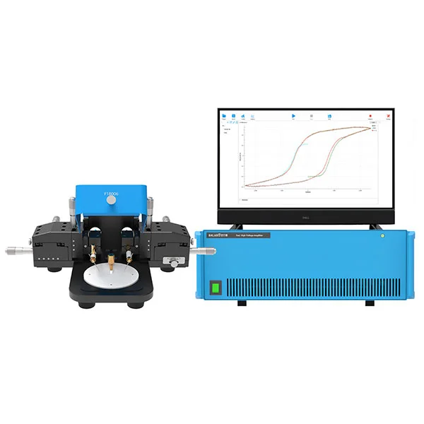
MatMeas FEAI1000 High-Precision Ferroelectric Analyzer
The MatMeas FEAI1000 is an advanced High-Precision Ferroelectric Analyzer specifically engineered for the rigorous evaluation of ferroelectric thin-film materials. Equipped with a built-in or external ±100V high-voltage amplifier, it delivers exceptional accuracy in measuring P-E hysteresis loops, spontaneous polarization, and leakage currents. Designed with proprietary high-voltage breakdown protection, it completely prevents the common catastrophic failures seen in traditional imported models. Offering measurement fidelity that directly rivals the German aixACCT TF2000 and surpassing the PolyK LY20, the FEAI1000 is the ultimate cost-effective infrastructure for dielectric functional ceramics research.
View details →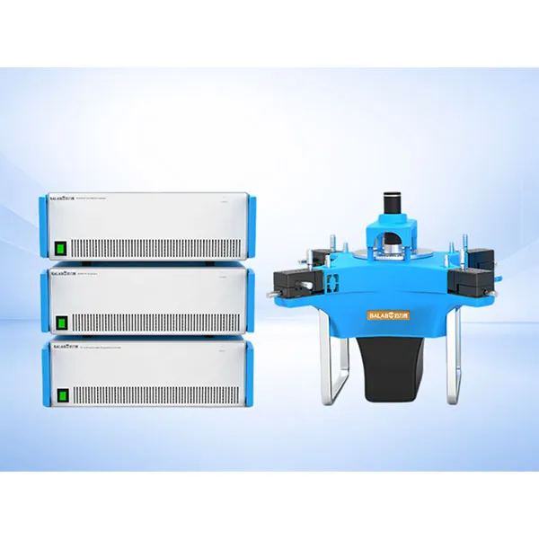
MatMeas FMS Ferroelectric Measurement Spectrometer
MatMeas High‑precision ferroelectric measurement system for hysteresis loop, fatigue testing and leakage current analysis under extreme temperatures.
View details →Request High-Precision Testing Solutions
Get expert guidance and customized instruments for your functional materials project.