Dielectric and Impedance Spectroscopy of Piezoelectric Thin Films
Technical News
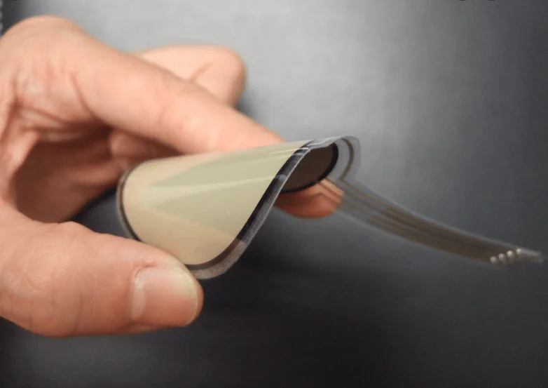
Piezoelectric thin films—primarily wurtzite aluminum nitride (AlN), transition-metal-doped scandium aluminum nitride (Al_1-x Sc_x N), lead zirconate titanate (PZT), and zinc oxide (ZnO)—are the foundational materials for radio-frequency (RF) acoustic filters, film bulk acoustic resonators (FBAR), solidly mounted resonators (SMR), and piezoelectric micromachined ultrasonic transducers (PMUT). In modern 5G/6G wireless communication transceivers and millimeter-wave front-end modules, these thin-film electro-acoustic devices operate at frequencies ranging from sub-gigahertz bands up to 10 GHz and beyond.
At these extreme frequencies, characterizing the dielectric and acoustic properties of sub-micron films presents severe metrological challenges. A piezoelectric thin film is not merely an electrical capacitor; it is an electro-acoustic transduction cavity bounded by metallic electrodes and a rigid substrate. The complex impedance response reflects a continuous interaction between dielectric displacement, acoustic wave propagation, acoustic reflection, electrode parasitic resistance, and interfacial space-charge trapping.
Accurately extracting the dielectric constant (epsilon_r'), loss tangent (tan delta), series resonance (f_s), parallel anti-resonance (f_p), effective electromechanical coupling factor (k_eff^2), and mechanical quality factor (Q_m) requires rigorous impedance modeling, Butterworth-Van Dyke (BVD) deconvolution, and fixture parasitic de-embedding in accordance with IEEE Std 176 and IEC 60250.
The Butterworth-Van Dyke (BVD) Acoustic Resonator Model
When an alternating electric field excites a piezoelectric thin-film resonator near its acoustic thickness-extensional mode, acoustic standing waves form between the top and bottom electrode interfaces. The resulting electrical impedance cannot be described by a passive capacitor; it must be modeled using the Butterworth-Van Dyke (BVD) equivalent circuit or its modified version (mBVD).
+---------------------------------------------------------------------------------------------------+
|                        Modified Butterworth-Van Dyke (mBVD) Circuit Model                        |
+---------------------------------------------------------------------------------------------------+
|                                                                                                   |
|               R_s (Electrode Series Resistance)       L_s (Lead Inductance)                       |
|        +-----[ R_s ]---------------------------------[ L_s ]----------------+                     |
|        |                                                                    |                     |
|        |      Static Capacitive Branch:                                     |                     |
|        +----+-----------------[ C_0 ]-----------------[ R_0 ]---------------+                     |
|        |    |                (Clamped)               (Dielectric            |                     |
|        |    |                                         Loss)                 |                     |
|        |    |                                                               |                     |
|        |    | Motional Acoustic Branch:                                     |                     |
|        |    +-----[ L_m ]------------[ C_m ]------------[ R_m ]-------------+                     |
|        |          (Acoustic           (Acoustic          (Mechanical        |                     |
|        |           Mass)              Elasticity)         Loss)             |                     |
|        |                                                                    |                     |
|        +--------------------------------------------------------------------+                     |
+---------------------------------------------------------------------------------------------------+
The mBVD model separates the total complex admittance Y(omega) into two parallel branches:
Y(omega) = Y_static(omega) + Y_motional(omega)
1. Static Branch (Dielectric Response)
The static branch represents the purely electrical clamped capacitance (C_0) of the thin film plus an effective parallel resistance (R_0) accounting for intrinsic dielectric loss:
Y_static(omega) = j * omega * C_0 / (1 + j * omega * C_0 * R_0) approx j * omega * C_0 + omega * C_0 * tan(delta_d)
Where C_0 = (epsilon_0 * epsilon33_S * A) / h, and epsilon33_S is the clamped (strain-free) relative permittivity.
2. Motional Branch (Acoustic Resonance)
The motional branch represents mechanical acoustic energy storage and dissipation within the vibrating film:
- L_m (Motional Inductance): Represents the effective acoustic mass or inertia of the vibrating piezoelectric layer: L_m = (rho * h^3) / (8 * A * e33^2), where rho is mass density and e33 is the piezoelectric stress constant.
- C_m (Motional Capacitance): Represents the mechanical elastic compliance of the film: C_m = (8 * A * e33^2) / (pi^2 * c33_D * h), where c33_D is the stiffened longitudinal elastic modulus.
- R_m (Motional Resistance): Represents acoustic energy loss resulting from viscous mechanical damping, grain boundary scattering, and acoustic radiation leakage into the substrate.
The total impedance across the motional branch is:
Z_motional(omega) = R_m + j * [omega * L_m - 1 / (omega * C_m)]
Resonance and Anti-Resonance Frequencies
The series resonance frequency (f_s, minimum electrical impedance, phase = 0) occurs when the motional inductance cancels the motional capacitance:
f_s = 1 / (2 * pi * sqrt(L_m * C_m)) = v_acoustic / (2 * h)
Where v_acoustic = sqrt(c33_D / rho) is the acoustic longitudinal phase velocity in the piezoelectric medium. The parallel anti-resonance frequency (f_p, maximum electrical impedance) occurs when the net motional inductance resonates with the parallel static capacitance C_0:
f_p = f_s * sqrt(1 + C_m / C_0)
Figures of Merit: Coupling Factor (k_eff^2) and Quality Factor (Q_m)
The operational bandwidth and insertion loss of RF acoustic filters are determined by two primary figures of merit extracted directly from impedance spectroscopy:
1. Effective Electromechanical Coupling Factor (k_eff^2)
Under the IEEE Std 176 standard formulation, the effective electromechanical coupling factor is calculated from the separation between resonance and anti-resonance frequencies:
k_eff^2 = (pi / 2) * (f_s / f_p) * cot((pi / 2) * (f_s / f_p))
For small frequency separations (f_p - f_s << f_s), this simplifies to the widely used standard approximation:
k_eff^2 approx (pi^2 / 4) * ((f_p - f_s) / f_p) approx (f_p^2 - f_s^2) / f_p^2
A larger frequency separation between f_s and f_p indicates superior electromechanical energy conversion, enabling wider filter passbands.
2. Mechanical Quality Factor (Q_m) and Resonator Figure of Merit (FoM)
The mechanical quality factor quantifies the sharpness of the acoustic resonance peak and is defined as the ratio of energy stored to energy dissipated per acoustic cycle:
Q_m = (2 * pi * f_s * L_m) / R_m = 1 / (2 * pi * f_s * C_m * R_m)
Experimentally, Q_m is extracted using the 3 dB bandwidth method or from the maximum slope of the input impedance phase angle (theta):
Q_m = (f_s / 2) * |d(theta) / df|_(f = f_s)
The overarching Figure of Merit (FoM) defining the performance envelope of a thin-film resonator technology is the product of coupling and quality:
FoM = k_eff^2 * Q_m
Material Technology Comparison: AlN, AlScN, PZT, and ZnO
The table below compiles physical and RF figures of merit for the leading piezoelectric thin-film technologies used in commercial and aerospace acoustic filter devices.
| Physical / Metrological Property | Pure AlN Thin Film | Scandium-Doped AlScN (Sc = 20-30%) | Lead Zirconate Titanate (PZT Thin Film) | Zinc Oxide (ZnO Thin Film) |
|---|---|---|---|---|
| Crystal Symmetry | Hexagonal Wurtzite (P6_3mc) | Wurtzite (softened lattice) | Perovskite (Tetragonal / Rhombohedral) | Hexagonal Wurtzite (P6_3mc) |
| Acoustic Velocity v_long (m/s) | 10,400 to 11,300 (ultra-fast) | 8,800 to 9,800 | 4,200 to 4,800 (slow velocity) | 6,000 to 6,400 |
| Relative Permittivity (epsilon_r) | 8.5 to 10.0 (low dielectric load) | 12.0 to 18.0 | 300 to 1,200 (very high) | 8.5 to 11.0 |
| Dielectric Loss Tangent (tan delta) | 0.001 to 0.003 (ultra-low loss) | 0.003 to 0.008 | 0.020 to 0.050 (lossy) | 0.005 to 0.015 |
| Piezoelectric Constant d33,f (pC/N) | 3.9 to 5.5 | 12.0 to 25.0 (dramatic boost) | 60.0 to 150.0 (enormous coupling) | 5.0 to 9.0 |
| Effective Coupling k_eff^2 (%) | 6.0% to 7.0% | 12.0% to 18.0% | 8.0% to 15.0% | 6.5% to 8.5% |
| Mechanical Quality Factor Q_m | 1,500 to 3,000 (exceptional Q) | 800 to 1,500 | 100 to 300 (severe acoustic damping) | 500 to 1,200 |
| Resonator Figure of Merit (FoM) | 90 to 210 | 120 to 250 | 15 to 45 (limited by damping) | 35 to 90 |
| Primary RF Filter Application | High-frequency 5G bands (n77, n79) | Wideband 5G Sub-6 GHz and Wi-Fi 6E/7 | Low-frequency PMUT and energy harvest | Legacy FBAR duplexers |
Fixture Parasitics, Contact Resistance, and De-Embedding Protocols
At RF and microwave frequencies, parasitic elements introduced by probe contacts, interconnect traces, and coaxial cables easily swamp the true response of the piezoelectric film.
Measured Impedance Transformation:
Z_measured = (R_contact + j * omega * L_lead) + [Z_film || (1 / (j * omega * C_pad))]
The table below outlines common high-frequency parasitics and their corrective de-embedding protocols.
| Parasitic Element | Physical Root Cause | Impact on Measured Spectrum | Engineering De-Embedding Technique |
|---|---|---|---|
| Series Contact Resistance (R_s) | Finite sheet resistance of thin metal electrodes (Au, Pt, Mo) | Lowers apparent Q_m; artificially broadens the series resonance dip | Measure open-short de-embedding test structures on the same wafer |
| Lead Parasitic Inductance (L_s) | Inductance of probe needles, bond wires, and micro-traces | Shifts f_s downward; introduces false parasitic resonances | Execute Open-Short-Load (OSL) calibration at the exact probe tips |
| Pad Shunt Capacitance (C_pad) | Capacitance between probe contact pads and grounded Si substrate | Artificially inflates static C_0, reducing apparent k_eff^2 | Fabricate "dummy" open pads on substrate; subtract pad admittance Y_pad |
| Substrate Acoustic Leakage | Acoustic wave energy radiating into the underlying silicon wafer | Creates spurious acoustic ripples; degrades parallel Q_p | Implement Bragg acoustic reflector mirrors (SMR) or deep Si etching (FBAR) |
| Thermal Frost / Moisture Film | Sub-zero testing under ambient air deposits ice on wafer surface | Massive false dielectric relaxation peak near 0 C; dampens Q | Execute cryogenic sweeps strictly inside a turbomolecular high-vacuum chamber |
Two-Step Open-Short De-Embedding Mathematics
To extract the intrinsic film admittance Y_intrinsic(omega) from raw two-port S-parameter measurements:
- Measure an Open Dummy Structure (fabricated on the same wafer with pads intact but piezoelectric resonator active area removed): Y_open(omega).
- Measure a Short Dummy Structure (pads shorted directly at the resonator boundary with thick metal): Z_short(omega).
- The intrinsic admittance of the device under test (DUT) is isolated:
Y_deembedded(omega) = [ (Y_measured - Y_open)^(-1) - (Y_short - Y_open)^(-1) ]^(-1)
Executing this de-embedding protocol strips away probe contact resistance and pad shunt capacitance, restoring the true intrinsic motional resistance R_m and uncorrupted quality factor Q_m.
Cryogenic and High-Temperature Spectroscopic Platforms
Investigating temperature coefficients of frequency (TCF), dielectric phase transitions, and thermal depoling requires robust environmental control. In RF filter engineering, the temperature coefficient of series resonance frequency (TCF_s) must be tightly controlled:
TCF_s = (1 / f_s) * (df_s / dT)
For uncompensated AlN films, TCF_s is typically -25 to -30 ppm/K, requiring integration of silicon dioxide (SiO2, which exhibits a positive TCF) compensation layers.
Evaluating these thermal coefficients down to deep cryogenic temperatures (-160 C) or up to elevated temperatures (+450 C) demands pristine atmospheric isolation. The MatMeas DMS-2000 High-Low Temperature Dielectric Spectrometer integrates a vacuum-sealed cryostat with automated liquid nitrogen cooling, completely eliminating moisture condensation and guaranteeing frost-free dielectric spectra across the entire temperature envelope.
For non-destructive, wafer-level characterization of microscopic FBAR resonators, PMUT arrays, and un-diced thin-film chips, the MatMeas CPS-7000 Cryogenic Vacuum Probe Station provides four ultra-precise micro-manipulated probe arms inside a high-vacuum chamber. Its proprietary built-in pneumatic anti-vibration damping platform isolates the probes from building and vacuum pump vibrations, preventing tip chatter and contact resistance fluctuations.
When evaluating high-temperature bulk piezoelectric substrates, packaging layers, or transducer arrays up to extreme temperatures, the MatMeas DMS-1000 High-Temperature Dielectric Spectrometer provides multi-sample screening up to 1000 C with 0.05% measurement precision.
Best-Practice Laboratory SOP for Thin-Film Impedance Spectroscopy
To obtain reproducible, audit-compliant impedance spectra of piezoelectric thin films, execute the following standardized procedure:
- Wafer and Test Structure Inspection:
- Inspect top and bottom electrode metallization under an optical microscope to confirm absence of pinholes or over-etched undercut margins.
- Verify that bottom electrode ground contact resistance is below 1 ohm.
- RF Probe Calibration (GSG Configuration):
- For frequencies above 10 MHz, utilize Ground-Signal-Ground (GSG) coplanar probes with calibrated pitch (e.g., 100 um to 250 um).
- Perform Short-Open-Load-Thru (SOLT) or Line-Reflect-Match (LRM) calibration on an impedance standard substrate (ISS) directly at the probe tip plane.
- Probe Landing Protocol:
- Align GSG probe tips over test pads under a high-magnification stereo microscope.
- Lower probes until initial electrical contact is established, then apply a controlled skate of 25 um to 50 um to break through native aluminum or gold surface oxide without puncturing the metal pad.
- Impedance Sweep Execution:
- Configure the vector network analyzer (VNA) or precision impedance analyzer with an RF power level between -10 dBm and 0 dBm to avoid non-linear electro-elastic saturation.
- Set intermediate frequency (IF) bandwidth sufficiently low (100 Hz to 1 kHz) to maximize dynamic range and signal-to-noise ratio.
- Sweep frequency through the anticipated acoustic resonance window with high point density (at least 1,601 points across the resonance span).
- mBVD Circuit Parameter Extraction:
- Identify series resonance (f_s, minimum |Z|) and parallel anti-resonance (f_p, maximum |Z|).
- Extract C_0 from the off-resonance low-frequency slope of imaginary admittance: C_0 = Im(Y) / (2 * pi * f).
Temperature Coefficients of Resonance and Acoustic Power Handling
In mobile RF front-end architectures, acoustic filters must maintain stable passband edges across ambient operating temperatures ranging from -40 C to +85 C. The primary metric quantifying thermal drift is the Temperature Coefficient of Frequency (TCF), defined separately for series resonance (TCF_s) and parallel anti-resonance (TCF_p):
TCF_s = (1 / f_s) * (df_s / dT) = (1 / v_acoustic) * (dv_acoustic / dT) - alpha_thermal
Where:
- v_acoustic: Longitudinal acoustic wave velocity, governed by the effective elastic stiffness c33_D.
- alpha_thermal: Linear thermal expansion coefficient along the thickness axis.
In pure wurtzite AlN, the elastic constant softens significantly with increasing temperature, resulting in an uncompensated TCF_s between -25 ppm/K and -32 ppm/K. Over an operating span of 100 K, an uncompensated 3.5 GHz n78 band filter shifts by more than 10 MHz, which can violate steep adjacent-channel rejection masks. To neutralize this drift, acoustic engineers integrate positive-TCF silicon dioxide (SiO2) temperature-compensation layers directly beneath the piezoelectric stack, leveraging the anomalous positive temperature coefficient of shear modulus in amorphous SiO2 to achieve near-zero net TCF (< +/-5 ppm/K).
Furthermore, when driven at high RF input power levels (> +30 dBm in mobile transmitters), piezoelectric thin films exhibit non-linear Duffing resonance shifts. High dynamic acoustic strain drives domain wall or lattice anharmonicity, causing the resonance peak to fold over toward lower frequencies (spring-softening behavior). Characterizing this non-linear impedance response as a function of continuous RF power is vital to guarantee that high-power transmit signals do not trigger intermodulation distortion (IMD) or premature acoustic fatigue failure.
Frequently Asked Questions (FAQ)
What is the difference between clamped permittivity (epsilon_S) and free permittivity (epsilon_T)?
At low frequencies (well below the fundamental acoustic resonance, f << f_s), the piezoelectric film is mechanically free to expand and contract in response to the applied electric field. Under this unconstrained boundary condition, the material exhibits its "free" relative permittivity (epsilon_T), which incorporates both pure dielectric polarization and piezoelectric strain coupling. At frequencies well above the acoustic resonance (f >> f_p), the mass inertia of the film prevents macroscopic mechanical deformation during rapid field reversals. The film is effectively mechanically clamped, exhibiting its "clamped" permittivity (epsilon_S):
epsilon33_S = epsilon33_T * (1 - k33^2)
Because the electromechanical coupling factor k33 is non-zero, the clamped permittivity is always strictly smaller than the free permittivity.
Why does the effective electromechanical coupling factor (k_eff^2) in thin-film FBARs differ from bulk k33?
Bulk electromechanical coupling factors (such as k33 or kt) represent ideal, intrinsic material properties measured on unconstrained, self-supporting single crystals or ceramics. In thin-film FBAR or SMR resonators, the effective coupling factor k_eff^2 is an extrinsic device-level metric. It is attenuated by acoustic energy stored in non-piezoelectric layers (such as top and bottom metal electrodes, adhesion interlayers, and underlying substrate Bragg mirrors), as well as lateral two-dimensional elastic clamping imposed by the rigid substrate wafer. Consequently, while intrinsic kt^2 for pure AlN is approximately 6.5%, an un-optimized FBAR device may exhibit a k_eff^2 of only 5.0% to 5.5%.
What causes spurious resonance peaks (ripples) near the main thickness-extensional mode?
Spurious resonance ripples occurring adjacent to the main acoustic thickness-extensional resonance originate from lateral transverse acoustic modes (Lamb waves and shear waves) propagating laterally along the substrate plane and reflecting off the electrode perimeter. These unwanted modes dissipate acoustic energy and distort passband flatness in RF filters. Engineers eliminate lateral spurious modes by designing apodized (non-parallel, pentagonal or irregular) top electrode geometries and etching acoustic border rings (frame structures) along the electrode periphery to suppress transverse acoustic leakage.
Related Instruments & Equipment
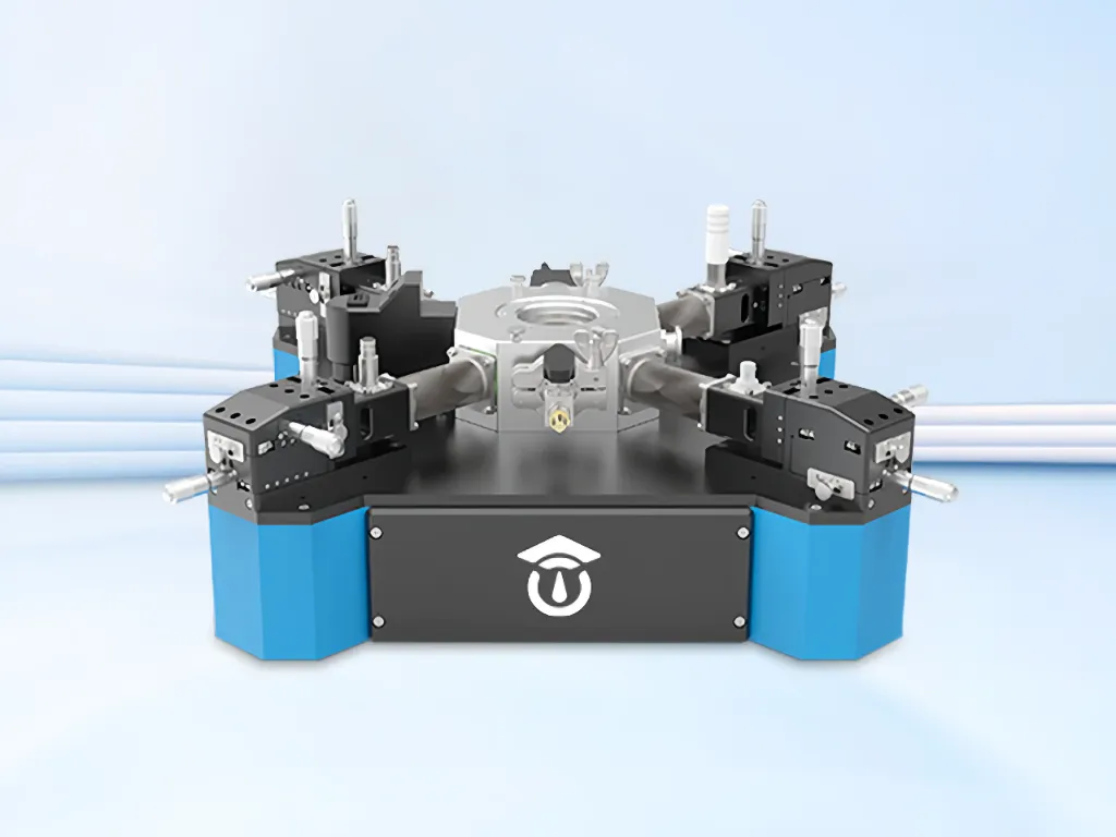
CPS7000 High-Low Temperature Dielectric Vacuum Probe Station
The MatMeas CPS7000 is an advanced, highly integrated desktop High-Low Temperature Dielectric Vacuum Probe Station engineered for the rigorous electrical characterization of thin films, bulk materials, and semiconductor wafers. Delivering performance directly comparable to industry-leading American brands like Lake Shore and Janis, this compact platform offers an ultra-wide temperature range from -160°C to 450°C via liquid nitrogen cooling. Uniquely equipped with a proprietary built-in air shock anti-vibration system, the CPS7000 eliminates data jumping points during continuous temperature variations. Supporting complex high-voltage and low-current testing environments, it is the ultimate infrastructure for evaluating dielectric, piezoelectric, ferroelectric, and TSDC properties in high-vacuum conditions.
View details →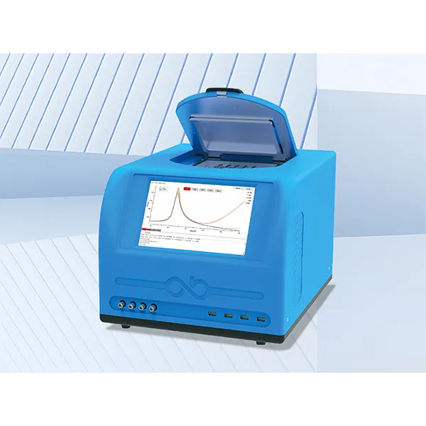
MatMeas DMS2000 High-Low Temperature Dielectric Spectrometer
The MatMeas DMS2000 is an advanced High and Low Temperature Dielectric Impedance Spectrometer engineered for evaluating the dielectric properties of materials under extreme thermal conditions. Compliant with the ASTM D150 standard, it integrates a proprietary LNP-95 liquid nitrogen injection system to achieve seamless continuous temperature variation from -160°C to 450°C. Uniquely featuring a vacuum-enabled sample chamber to completely prevent thermal frosting and eliminate false water peaks near 0°C, along with versatile options for single-sample or five-sample simultaneous testing, the DMS2000 ensures unparalleled data fidelity and high throughput for advanced scientific research.
View details →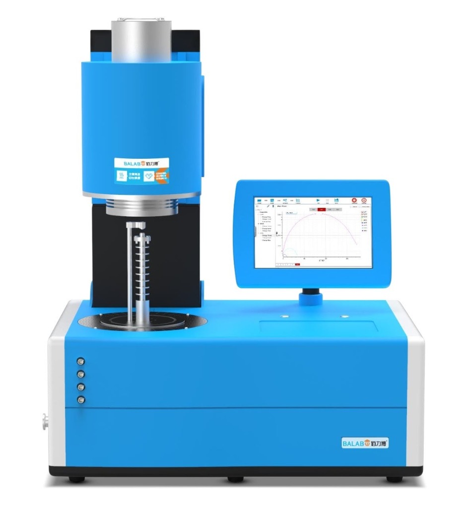
MatMeas DMS1000 High-Temperature Dielectric Spectrometer
The MatMeas DMS1000 is an advanced High-Temperature Dielectric Impedance Temperature Spectrometer engineered for the ultimate electrical characterization of bulk materials. Delivering an exceptional measurement accuracy of 0.05%, it operates efficiently from Room Temperature (RT) to 1000°C. Its upgraded platform supports both single-sample and four-sample simultaneous measurements. Integrated with a sealable metal shielding system and high-purity platinum electrodes, the DMS1000 enables highly reliable testing across inert, oxidizing, reducing, and vacuum atmospheres, making it an indispensable infrastructure for precision materials science.
View details →Request High-Precision Testing Solutions
Get expert guidance and customized instruments for your functional materials project.