Room-Temperature d33 Testing of Piezoelectric Thin Films
Technical News
The longitudinal piezoelectric charge coefficient (d33) defines the electric polarization charge density generated along the polar z-axis per unit of mechanical compressive stress applied collinearly along that same direction. In macroscopic, freestanding bulk ceramics, d33 represents an unconstrained material tensor parameter. In functional thin films—such as lead zirconate titanate (PZT), aluminum nitride (AlN), scandium-doped AlScN, and lead-free perovskites grown on thick silicon, sapphire, or glass wafers—the measured longitudinal piezoelectric response is fundamentally different from that of bulk ceramics.
Because the underlying substrate is typically several hundred micrometers thick (e.g., 500 um silicon) while the active piezoelectric film is sub-micron to a few micrometers in thickness (0.1 um to 2 um), the substrate rigidly clamps the film in the two-dimensional lateral plane. Under applied axial force or through-thickness electric fields, the film is mechanically constrained from undergoing lateral Poisson contraction or expansion. Consequently, the experimentally observed parameter is an effective thin-film piezoelectric coefficient, formally designated as d33,f.
Characterizing d33,f with metrological rigor requires applying the Lefki-Dormans elastic clamping correction, decoupling bending-mode flexoelectric artifacts, optimizing contact probe tip geometry, and selecting appropriate testing platforms in accordance with IEEE Std 176 and SEMI MS4-0307.
Elastic Substrate Clamping Mechanics: The Lefki-Dormans Formalism
In unconstrained bulk piezoelectric ceramics, applying an axial stress (T3) induces both longitudinal strain (S3 = s33_E * T3) and lateral transverse strain (S1 = S2 = s13_E * T3) through elastic Poisson coupling. In a thin film rigidly bonded to a thick substrate, the zero-slip interfacial boundary condition forces the in-plane strains to zero (S1 = S2 = 0) at the film-substrate interface.
+---------------------------------------------------------------------------------------------------+
|                        Substrate Clamping and Lateral Stress Induction                            |
+---------------------------------------------------------------------------------------------------+
|                                                                                                   |
|             Applied Axial Stress T3 (Direct) or Electric Field E3 (Converse)                      |
|                                         |                                                         |
|                                         v                                                         |
|           +---------------------------------------------+  Top Electrode                          |
|  Clamped  |      <--- In-Plane Stress T1, T2 --->       |                                         |
|  Active   |             T1 = T2 = - (s13/s11+s12) * T3  |  Piezoelectric Film (h ~ 1 um)          |
|  Layer    |      <--- Substrate Resists Lateral Motion  |                                         |
|           +---------------------------------------------+  Bottom Electrode                       |
|           |                                             |                                         |
|           |         Rigid Substrate (H ~ 500 um)        |  Zero In-Plane Strain (S1 = S2 = 0)     |
|           +---------------------------------------------+                                         |
+---------------------------------------------------------------------------------------------------+
Under this two-dimensional mechanical constraint, longitudinal deformation induces large reactive in-plane stresses (T1 and T2). Setting in-plane strains to zero in the general electro-elastic compliance tensor yields:
S1 = s11_E * T1 + s12_E * T2 + s13_E * T3 + d31 * E3 = 0
For an isotropic in-plane crystal texture (T1 = T2), the induced reactive lateral stress is:
T1 = T2 = - [s13_E / (s11_E + s12_E)] * T3 - [d31 / (s11_E + s12_E)] * E3
Substituting this reactive stress into the longitudinal displacement equation (D3 = d31 * (T1 + T2) + d33 * T3 + epsilon33_T * E3) yields the constitutive equation for the effective thin-film piezoelectric coefficient (d33,f), derived by Lefki and Dormans:
d33,f = d33 - [2 * s13_E / (s11_E + s12_E)] * d31
In terms of the thin film's in-plane Poisson's ratio (nu = - s13_E / (s11_E + s12_E)) and Young's modulus (Y = 1 / s11_E):
d33,f = d33 - [2 * nu / (1 - nu)] * d31
Because the transverse piezoelectric coefficient d31 possesses the opposite sign of d33 in most perovskite and wurtzite ferroelectrics (e.g., in PZT, d33 is positive while d31 is negative; d31 approx -0.4 * d33), the clamping term subtracts from the intrinsic response:
- For bulk PZT-5H: d33 approx 600 pC/N, d31 approx -260 pC/N, nu approx 0.35.
- Calculated effective thin-film coefficient: d33,f = 600 - [2 * (0.35) / (1 - 0.35)] * (-260) = 600 - (1.077 * 260) approx 60 to 120 pC/N.
Substrate clamping diminishes the observable longitudinal piezoelectric charge output of PZT films by 60% to 80% compared to freestanding bulk ceramics. In AlN films where d33 is approx +5.5 pC/N and d31 is approx -2.5 pC/N, d33,f drops to 3.8 to 4.5 pC/N. Reporting d33 values for thin films without explicitly indicating whether the figure represents intrinsic bulk d33 or clamped effective d33,f invalidates engineering models.
Metrological Methodologies: Direct versus Converse Characterization
Characterizing d33,f in thin films relies on two complementary physical phenomena:
Direct Method (Direct Piezoelectric Effect):
Apply Dynamic Force delta_F ---> Measure Collected Charge Q ---> d33,f = Q / delta_F

Converse Method (Converse Piezoelectric Effect):
Apply AC Voltage V_exc ---> Measure Surface Displacement delta_h ---> d33,f = delta_h / V_exc
+---------------------------------------------------------------------------------------------------+
|                        Thin-Film d33,f Characterization Techniques                                |
+---------------------------------------------------------------------------------------------------+
|  [1. Direct Dynamic Micro-Force Method (Berlincourt-Type / PEAI-1000)]                            |
|  Applies calibrated dynamic uniaxial force normal to top electrode; measures charge via lock-in.  |
|                                                                                                   |
|  [2. Double-Beam Laser Interferometer (DBLI)]                                                     |
|  Directly measures converse out-of-plane displacement (delta_h) on top surface while subtracting  |
|  substrate rear-surface displacement to eliminate wafer bending.                                  |
|                                                                                                   |
|  [3. Laser Doppler Vibrometer (LDV)]                                                              |
|  High-frequency optical Doppler shift of reflected laser beam; sensitive to substrate bending.    |
|                                                                                                   |
|  [4. Piezoresponse Force Microscopy (PFM)]                                                        |
|  Conductive AFM tip applies localized field and measures picometer deflection; nanoscale mapping. |
+---------------------------------------------------------------------------------------------------+
1. Direct Dynamic Micro-Force Method
The direct method exerts a cyclic compressive force F(t) = F_static + delta_F * sin(omega * t) normal to the film surface using a calibrated mechanical probe. The induced charge Q(t) is collected across the film thickness and routed to a virtual-ground charge integrator:
Q(t) = d33,f * delta_F * sin(omega * t)
The primary experimental hurdle is the elimination of wafer flexure. If the loading tip exerts force on a thin film supported by an unbacked wafer, the entire substrate flexes like a mechanical diaphragm. This flexural strain induces enormous transverse piezoelectric charges via d31 coupling:
Q_measured = d33,f * F_axial + d31_eff * F_bending
In un-optimized test rigs, flexural d31 charges can be 5 to 10 times larger than the true d33,f charge, reversing the apparent signal polarity or artificially inflating d33,f. To eliminate bending artifacts, the substrate must be mounted on an optically flat, rigid tungsten carbide anvil, or loaded with identical, aligned opposed coaxial tips on both faces.
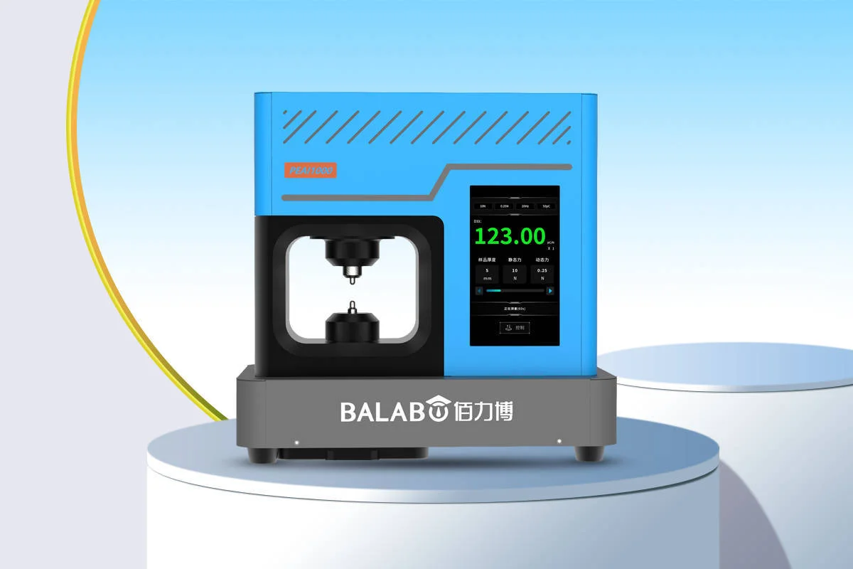
The MatMeas PEAI-1000 High-Precision Piezoelectric Analyzer resolves this with automated coaxial tip alignment and precise micro-force control, maintaining static preloads (1 N to 10 N) and dynamic forces (0.05 N to 0.5 N) to eliminate bending modes while avoiding crushing delicate sub-micron films.
2. Converse Double-Beam Laser Interferometry (DBLI)
In converse testing, an AC voltage V(t) = V_0 * sin(omega * t) is applied across the film thickness, generating longitudinal strain (S3 = delta_h / h = d33,f * E3 = d33,f * V_0 / h). The resulting surface displacement (delta_h) is independent of film thickness:
delta_h = d33,f * V_0
For a typical 1 V excitation, AlN produces delta_h approx 4.0 picometers, while PZT produces delta_h approx 80 to 120 picometers. Single-beam interferometers or laser vibrometers mistake substrate flexure for true thickness expansion. The Double-Beam Laser Interferometer (DBLI) splits a coherent laser beam into two arms: one beam reflects off the top electrode of the film, while the second reflects off the backside of the substrate directly beneath the excitation spot. Optically subtracting backside displacement eliminates wafer bending, isolating pure longitudinal thickness dilation.
Metrological Comparison Matrix: Thin-Film d33,f Characterization Techniques
The table below contrasts the four primary experimental techniques used to quantify effective thin-film piezoelectric coefficients.
| Metrological Parameter | Direct Dynamic Micro-Force (PEAI-1000) | Double-Beam Laser Interferometry (DBLI) | Single-Beam Laser Doppler Vibrometer (LDV) | Piezoresponse Force Microscopy (PFM) |
|---|---|---|---|---|
| Physical Effect | Direct piezoelectric effect (charge from force) | Converse effect (displacement from voltage) | Converse effect (surface velocity/displacement) | Converse effect (localized AFM tip deflection) |
| Excitation Signal | Cyclic force (0.05 N to 0.5 N, 30–300 Hz) | AC voltage (0.1 V to 10 V, 1 kHz to 50 kHz) | High-frequency AC voltage (10 kHz to 10 MHz) | Localized AC voltage applied through AFM tip |
| Measured Observable | Generated charge Q (pC) via virtual ground TIA | Optical interference fringe phase shift (pm) | Doppler frequency shift of reflected beam | Photodiode cantilever deflection voltage |
| Spatial Resolution | Macro-scale (defined by electrode: 0.5–5 mm) | Macro-to-micro (laser spot diameter: ~50 um) | Micro-scale (focused spot: ~5 to 20 um) | Nanoscale (AFM tip radius: 10 to 30 nm) |
| Wafer Bending Immunity | High when rigid flat anvil backing is used | Complete; optical differential cancellation | None; heavily corrupted by flexural modes | High; tip interaction is localized to nano-volume |
| Quantitative Accuracy | High (+/-2% with calibrated force sensor) | High (+/-5% absolute optical calibration) | Semi-quantitative; requires de-embedding | Qualitative to semi-quantitative (tip-field error) |
| Sample Preparation | Standard top/bottom metallized film chip | Highly reflective top electrode and polished rear | Highly reflective patterned micro-electrodes | Exposed conductive top electrode or bare film |
| Measurement Speed | Rapid (<30 seconds per test point) | Slow (requires precise dual-beam alignment) | Moderate (optical focusing required) | Very slow (raster scanning across area) |
Contact Mechanics: Hertzian Stress and Preload Optimization
When conducting direct micro-force d33,f measurements, the mechanical interface between the loading tip and the top metal electrode is governed by Hertzian contact mechanics.
+---------------------------------------------------------------------------------------------------+
|                        Hertzian Contact Mechanics at Film Interface                               |
+---------------------------------------------------------------------------------------------------+
|                                                                                                   |
|                       Applied Preload Force F_preload                                             |
|                                     |                                                             |
|                                     v                                                             |
|                              /-------------\                                                      |
|                             /  Spherical    \  Radius R_tip (Sapphire / WC)                       |
|                            (   Loading Tip   )                                                    |
|                             \               /                                                     |
|                              \---+-+-+-+---/                                                      |
|                                    | | |                                                          |
|       +----------------------------+-+-+----------------------------+ Top Electrode               |
|       |  * * * * * * * * * * * * [a_contact] * * * * * * * * * * *  |                             |
|       |     Maximum Compressive Stress:                             | Piezoelectric Film (h)      |
|       |     sigma_0 = (3 * F_preload) / (2 * pi * a_contact^2)      |                             |
|       +-------------------------------------------------------------+ Bottom Electrode            |
+---------------------------------------------------------------------------------------------------+
For a spherical contact tip of radius R_tip pressed against an elastic half-space with effective modulus E*, the circular contact radius a_contact is:
a_contact = [ (3 * F_preload * R_tip) / (4 * E*) ]^(1 / 3)
The maximum compressive stress (sigma_0) developed at the center of the contact circle is:
sigma_0 = (3 * F_preload) / (2 * pi * a_contact^2)
This contact mechanics formulation establishes two critical boundaries:
- Puncture and Micro-Cracking Threshold: If a sharp needle tip (R_tip < 100 um) is used with a heavy preload (e.g., 5 N), the localized contact stress easily exceeds 5 GPa. This extreme stress pierces through the thin metal electrode, micro-cracks brittle oxide films (like PZT), and creates electrical short circuits.
- Stress Homogeneity: If the contact radius a_contact is much smaller than the top electrode diameter, the stress distribution underneath the electrode is non-uniform, requiring integration of the localized stress tensor.
To ensure uniform stress transfer without mechanical damage, loading tips must utilize polished spherical geometries (R_tip between 2 mm and 10 mm) manufactured from ultra-hard sapphire or tungsten carbide, with static preloads calibrated between 0.5 N and 2.0 N.
Benchmark Parameters across Thin-Film Families
The table below summarizes typical effective thin-film piezoelectric coefficients (d33,f) alongside their bulk counterparts and elastic constants.
| Thin-Film Material System | Deposition Technique | Film Thickness Range | Intrinsic Bulk d33 (pC/N) | Clamped Thin-Film d33,f (pC/N) | In-Plane Poisson's Ratio (nu) | Clamping Reduction Factor |
|---|---|---|---|---|---|---|
| Pure Wurtzite AlN | Pulsed DC Magnetron Sputtering | 0.5 to 2.0 um | +5.5 | +3.8 to +4.8 | 0.24 to 0.28 | ~20% reduction |
| Al_0.7 Sc_0.3 N Alloy | Co-Sputtering (Al + Sc targets) | 0.5 to 1.5 um | +28.0 | +18.0 to +24.0 | 0.30 to 0.34 | ~25% reduction |
| Sol-Gel PZT (52/48 MPB) | Spin-Coating / Rapid Thermal Anneal | 0.2 to 2.0 um | +650 | +80 to +130 | 0.35 to 0.38 | ~80% reduction |
| Sputtered PZT Thin Film | RF Magnetron Sputtering (Pt/Si) | 1.0 to 4.0 um | +500 | +60 to +110 | 0.35 to 0.38 | ~82% reduction |
| Barium Titanate (BaTiO3) | Pulsed Laser Deposition (PLD) | 0.1 to 0.5 um | +190 | +25 to +45 | 0.32 to 0.35 | ~80% reduction |
| PVDF-TrFE Copolymer | Spin-Coating / Thermal Anneal | 1.0 to 10.0 um | -33.0 | -15.0 to -22.0 | 0.38 to 0.42 | ~40% reduction |
Comprehensive In-Situ Dynamic and Resonance Platforms
In advanced device qualification, static room-temperature measurements must be complemented by thermal sweeps and high-frequency resonance mapping. As operational temperatures fluctuate, thermal expansion mismatches between film and substrate alter in-plane clamping stresses, shifting the effective d33,f.
The MatMeas PEMS-1000 In-Situ Dynamic Piezoelectric System provides dynamic frequency sweeping (30 Hz to 300 Hz) and in-situ thermal tracking. Its closed-loop lock-in amplification isolates minute displacement charges from ambient thermal drift and DC pyroelectric currents, ensuring reproducible dynamic d33,f tracking up to 800 C.
For complete electromechanical parameter extraction—including transverse d31 coupling, thickness-shear d15 coefficients, and planar coupling factors (k_p)—the MatMeas PCA-1000 Piezoelectric Characterization Analyzer provides automated resonance and anti-resonance tracking in accordance with IEEE Std 176 and MIL-STD-1376.
For fragile sub-micron films requiring non-destructive, room-temperature screening, the MatMeas PEAI-1000 High-Precision Piezoelectric Analyzer provides calibrated servo-controlled micro-force clamping, preventing film punch-through while delivering high-accuracy d33,f measurements across an ultra-wide 0 to 2000 pC/N dynamic range.
Best-Practice Laboratory SOP for Thin-Film d33,f Testing
To ensure peer-reviewed reproducibility in direct micro-force d33,f characterization:
- Substrate Backing and Planarity:
- Clean the substrate backside to remove silicon dust or particulate contamination.
- Mount the specimen onto a rigid, polished anvil (surface roughness Ra < 0.1 um) using a sub-micron film of low-viscosity cyanoacrylate or vacuum clamping to eliminate flexural compliance.
- Electrode Integrity Verification:
- Inspect top circular electrode pads (diameter 1.0 mm to 2.0 mm) under an optical microscope.
- Confirm that top electrode sheet resistance is below 5 ohms/sq and bottom electrode ground return is verified.
- Preload Engagement:
- Align the spherical sapphire loading tip (radius R = 3.0 mm) with the exact center of the metallized pad.
- Lower the actuator until a static preload force F_preload = 1.00 N (+/-0.05 N) is registered by the in-line load cell.
- Dwell for 30 seconds to allow mechanical relaxation of fixture mounts.
- Dynamic Force Calibration:
- Apply a sinusoidal dynamic force delta_F = 0.20 N RMS at a frequency of 110 Hz.
- Monitor the dynamic force load cell output on an oscilloscope to confirm zero harmonic distortion and verify that total force never drops below 0.5 N (preventing tip chattering).
- Phase-Locked Charge Measurement:
- Route collected charge through a low-noise virtual-ground transimpedance preamplifier.
- Demodulate the charge signal using a lock-in amplifier referenced to the 110 Hz shaker drive frequency.
- Reverse the electrical polarity of the probe connections or flip the sample orientation to verify an exact 180-degree phase shift, confirming that the acquired signal is genuine piezoelectricity rather than electromagnetic pickup.
- Data Reporting:
- Calculate d33,f = Q_rms / delta_F_rms.
- Report film thickness, substrate material, electrode diameter, static preload force, dynamic force amplitude, excitation frequency, and the resulting d33,f value.
Frequently Asked Questions (FAQ)
Why is the measured d33 of a PZT thin film so much lower than bulk PZT ceramic?
In bulk PZT ceramics, grains are free to expand laterally when compressed axially, allowing full 90-degree and 180-degree domain wall motion that produces high d33 values (400 to 600 pC/N). When deposited as a thin film on a thick silicon or sapphire substrate, the rigid substrate clamps the in-plane dimensions (S1 = S2 = 0). Compressing the film axially attempts to expand it laterally, which is resisted by the substrate, generating intense in-plane compressive stresses (T1 and T2). Via transverse d31 coupling, this reactive stress generates opposing charges that cancel out a major portion of the longitudinal charge: d33,f = d33 - [2 * nu / (1 - nu)] * d31. Substrate clamping reduces the apparent d33 of PZT films to 60–120 pC/N.
How can one experimentally prove that a d33 measurement is free of wafer bending artifacts?
Wafer flexural bending introduces parasitic transverse charges via d31 that corrupt direct d33 measurements. To prove the absence of bending artifacts:
- Varying Substrate Thickness: Measure identical films deposited on substrates of different thicknesses (e.g., 300 um, 500 um, 1000 um Si). If bending artifacts are present, measured d33 will vary inversely with substrate flexural rigidity (scaling with substrate thickness cubed, H^3). In a properly backed, bending-free test setup, measured d33,f remains completely invariant across all substrate thicknesses.
- Double-Sided opposed loading: Loading the sample symmetrically with two identical opposed coaxial tips cancels bending moments.
- Phase Inversion Check: Reversing the poling orientation of the film must invert the output phase by exactly 180 degrees without altering magnitude.
What is the advantage of using spherical loading tips over flat punch tips?
Flat punch tips require absolute parallelism between the punch face and the specimen surface. A misalignment of merely 0.05 degrees causes the sharp edge of a flat punch to dig into the thin film, creating extreme localized stress concentrations, micro-cracking, and punch-through short circuits. Spherical tips (radii 2 mm to 5 mm) ensure smooth Hertzian contact that is self-centering and completely immune to minor angular misalignments, establishing a predictable, reproducible stress profile without cutting the metal electrode.
Related Instruments & Equipment
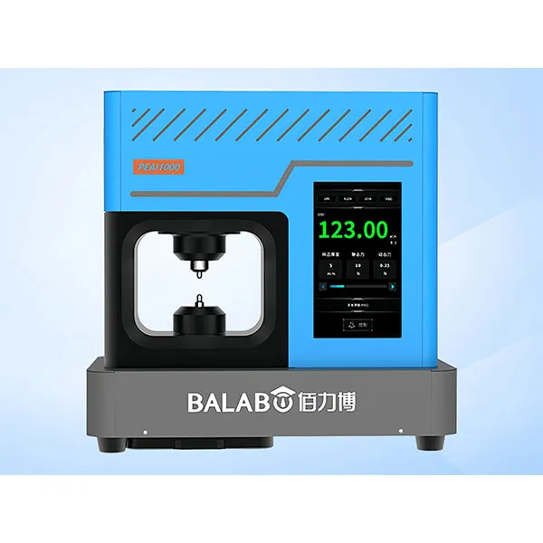
MatMeas PEAI1000 High-Precision Piezoelectric Analyzer
The MatMeas PEAI1000 is a next-generation High-Precision Piezoelectric Analyzer engineered to evaluate the piezoelectric coefficient (d33) of advanced functional materials. Surpassing the limitations of traditional d33 measuring instruments, it employs an advanced dynamic measurement method integrated with cutting-edge lock-in amplification technology. This architecture strictly suppresses environmental noise, significantly improving the signal-to-noise ratio. Capable of applying variable static clamping forces (1~10N) and precise dynamic test forces (0.1~0.5N), it guarantees an ultra-wide measurement range (0 to 2000 pC/N) with an exceptional accuracy of ±2%. It is an essential, highly reliable tool for the research, application, and mass production of piezoelectric blocks, plates, and delicate thin films.
View details →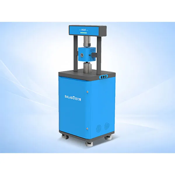
MatMeas High Precision In‑situ d33 Piezoelectric Measurement System – PEMS Analyzer
MatMeas PEMS is a high‑precision in‑situ d33 piezoelectric measurement system for advanced material characterization.
View details →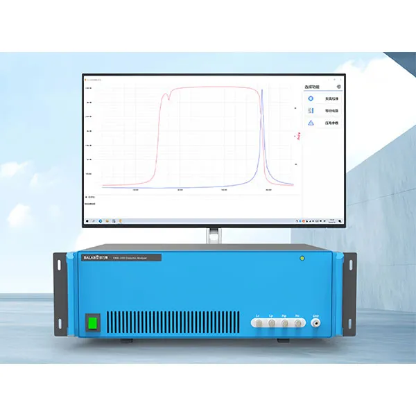
MatMeas High Precision Piezoelectric Ceramic Parameter Analyzer PCA1000
The MatMeas PCA1000 is a domestic-first, cutting-edge Piezoelectric Ceramic Integrated Analyzer engineered to comprehensively evaluate the performance of piezoelectric materials using the advanced AC resonance method. Operating across a wide frequency range from 20Hz to 10MHz with a high measurement accuracy of ±0.05%, it eliminates complex manual calculations by instantly extracting critical data, including electromechanical coupling coefficients (Kp, Kt), mechanical quality factors (Qm), piezoelectric constants (d33, d31, d15), and equivalent circuit models. With intelligent frequency sweeping and visualized data interfaces, the PCA1000 is the ultimate one-stop solution for both rigorous academic research and high-throughput quality screening in industrial mass production.
View details →Request High-Precision Testing Solutions
Get expert guidance and customized instruments for your functional materials project.