Alumina Ceramic Substrate Inspection & Testing Guide
Technical News
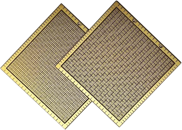
Polycrystalline alumina (aluminum oxide, Al2O3) substrates represent the foundational ceramic packaging and carrier platform for automotive power electronic modules (IGBTs, SiC MOSFETs), high-density thick-film hybrid integrated circuits (HICs), multi-chip modules (MCMs), and LED packaging. Offering an exceptional combination of electrical volume resistivity (>10¹⁴ Ω·cm at 25°C), high dielectric breakdown strength (>15 kV/mm), robust mechanical flexural strength (>350 MPa), and competitive manufacturing cost, alumina substrates provide essential electrical isolation while dissipating heat generated by active semiconductor junctions.
However, industrial quality control teams and module reliability engineers frequently encounter unexpected electrical and thermal failures. These failures originate from subtle variations in alumina purity grades—predominantly the distinction between 96% Al2O3 (liquid-phase sintered with silicate sintering aids) and 99.6% Al2O3 (solid-state sintered high-purity ceramic). At elevated operating temperatures (>300°C), alkali metal impurities and intergranular glassy phases dramatically lower volume resistivity, accelerating dielectric leakage and thermal breakdown, as quantified in dedicated alumina ceramic substrate high-temperature resistance testing. Establishing rigorous inspection and testing protocols conforming to international standards is vital to prevent catastrophic field failures.
Microstructural Conduction Physics and High-Temperature Resistivity Degradation
The electrical resistivity of polycrystalline alumina is fundamentally governed by its intergranular grain boundary chemistry. While pristine single-crystal corundum (sapphire, α-Al2O3) is an exceptional wide-bandgap electrical insulator with a bandgap Eg ≈ 8.8 eV, commercial polycrystalline substrates contain grain boundaries populated by sintering aids and residual impurities:
- 96% Alumina Formulation: Sintered at approximately 1550°C using liquid-phase sintering aids comprising silica (SiO2), calcia (CaO), and magnesia (MgO). Upon cooling, these additives precipitate as an amorphous calcium-magnesium-aluminosilicate glass network that wets and coats the crystalline α-Al2O3 grain boundaries.
- 99.6% Alumina Formulation: Sintered via solid-state diffusion at ~1650°C with minute MgO dopant additions (typically <0.1 wt%) to control grain boundary mobility. This results in direct grain-to-grain contact with negligible intergranular amorphous glassy phases.
At elevated operating temperatures (T > 300°C), electrical conduction through the continuous amorphous grain boundary network is activated by the thermal migration of mobile alkali metal ions (Na⁺, K⁺) and divalent alkaline earth cations (Ca²⁺, Mg²⁺). The temperature dependence of volume resistivity ρv follows the Arrhenius ionic conduction relation:
ρv(T) = ρ0 · exp[Ea / (kB · T)]
where ρ0 is the pre-exponential resistivity coefficient, Ea is the thermal activation energy for ionic hopping (typically 0.8 to 1.1 eV in 96% alumina glass phases, compared to 1.4 to 1.8 eV in high-purity 99.6% alumina), kB is the Boltzmann constant, and T is absolute temperature in Kelvin.
Consequently, while 96% and 99.6% alumina exhibit comparable room-temperature resistivity (ρv ≈ 10¹⁴ Ω·cm), at 600°C the volume resistivity of 96% alumina drops by up to six orders of magnitude (down to 10⁸ Ω·cm), whereas high-purity 99.6% alumina preserves a robust resistivity >10¹¹ Ω·cm.
Under a guarded triaxial parallel-plate electrode geometry conforming to ASTM D257, volume resistivity is extracted from measured insulation resistance Rv:
ρv = Rv · (Aeff / t) = Rv · [π · (D1 + g)² / (4 · t)]
where D1 is the guarded electrode diameter, g is the guard ring gap width, and t is the substrate tile thickness.
Comprehensive Benchmark: 96% vs. 99.6% Alumina Substrates
Selecting the correct alumina substrate grade requires balancing electrical insulation, thermal conductivity, surface micro-roughness, and metallization adhesion.
The benchmark table below compares physical, thermal, and electrical performance parameters across the two primary commercial alumina purity grades:
| Material Property Dimension | Standard Test Method | 96% Commercial Alumina (Thick-Film) | 99.6% High-Purity Alumina (Thin-Film) | Engineering Performance Impact |
|---|---|---|---|---|
| Al2O3 Purity Content | Chemical ICP-OES | 95.5% to 96.5% | 99.5% to 99.8% | High purity eliminates mobile alkali ion leakage paths |
| Secondary Glass Phase Fraction | SEM-EDS / XRD | 3.5 to 4.5 wt% (silicate glass) | < 0.2 wt% (direct grain contact) | Glass phase dictates high-temperature electrical degradation |
| Bulk Sintered Density | ASTM C373 | 3.75 to 3.82 g/cm³ | 3.90 to 3.96 g/cm³ | Higher density eliminates moisture-absorbing open porosity |
| Surface Roughness Ra (As-Fired) | Contact Profilometry | 0.3 to 0.6 μm | 0.05 to 0.12 μm | Smooth surface enables high-definition thin-film photolithography |
| Thermal Conductivity κ (25°C) | Laser Flash (ASTM E1461) | 22 to 25 W/m·K | 30 to 35 W/m·K | 40% higher heat dissipation in high-power modules |
| Volume Resistivity ρv (25°C) | ASTM D257 (500 V DC) | > 10¹⁴ Ω·cm | > 10¹⁵ Ω·cm | Both grades provide excellent room-temperature isolation |
| Volume Resistivity ρv (500°C) | ASTM D1829 (500 V DC) | 10⁸ to 10⁹ Ω·cm | 10¹¹ to 10¹² Ω·cm | 99.6% grade prevents thermal runaway in high-temp power circuits |
| Dielectric Strength Eb (0.635 mm) | ASTM D149 (Short-Time DC) | 15 to 18 kV/mm | 22 to 26 kV/mm | High dielectric barrier prevents electrical punch-through |
| Dielectric Loss tan δ (1 MHz, 25°C) | ASTM D150 | 3.0 to 6.0 × 10⁻⁴ | 0.8 to 1.5 × 10⁻⁴ | 99.6% grade suppresses signal attenuation in microwave circuits |
International Inspection Standards and Failure Mode Diagnostics
Comprehensive quality assurance of electronic ceramic substrates requires multi-parametric evaluation under international standards, systematically integrated within our advanced ceramic substrate electrical testing guide:
- ASTM D1829: Standard Test Method for Electrical Resistance and Resistivity of Ceramic Materials at Elevated Temperatures.
- ASTM D257: Standard Test Methods for DC Resistance or Conductance of Insulating Materials.
- ASTM D149: Standard Test Method for Dielectric Breakdown Voltage and Dielectric Strength of Solid Electrical Insulating Materials at Commercial Power Frequencies.
- IEC 60672: Specification for Ceramic and Glass Insulating Materials.
The diagnostic matrix below outlines common substrate failure modes encountered in power electronic packaging and their root-cause resolutions:
| Substrate Failure Mode | Underlying Root Cause | Electrical / Visual Symptom | Quality Control Inspection Protocol |
|---|---|---|---|
| High-Temp Leakage Current Spike | Alkali metal contamination (Na⁺, K⁺) in grain boundary glass | Sudden current increase at >300°C; low volume resistivity | Execute ASTM D1829 volume resistivity screening at 500°C |
| Dielectric Puncture Breakdown | Internal closed pores or metallic iron (Fe) inclusions from ball milling | Localized arc crater; pinhole punch-through under 5 kV DC | Screen with automated high-voltage hi-pot testing at 1.5× rated field |
| Edge Flashing / Creeping Arc | Inadequate creepage distance or surface moisture contamination | Carbonized surface tracking; arc across ceramic perimeter | Implement ASTM D149 dielectric breakdown testing per our ceramic substrate breakdown testing guide |
| Thin-Film Metallization Peeling | High surface roughness (Ra > 0.3 μm) or silicate glass segregations | Sputtered Au/Ti peel-off during scotch tape or ultrasonic pull test | Atomic force microscopy (AFM) surface roughness screening; switch to 99.6% Al2O3 |
Advanced High-Temperature High-Resistance Metrology: MatMeas HTS-1000HR System
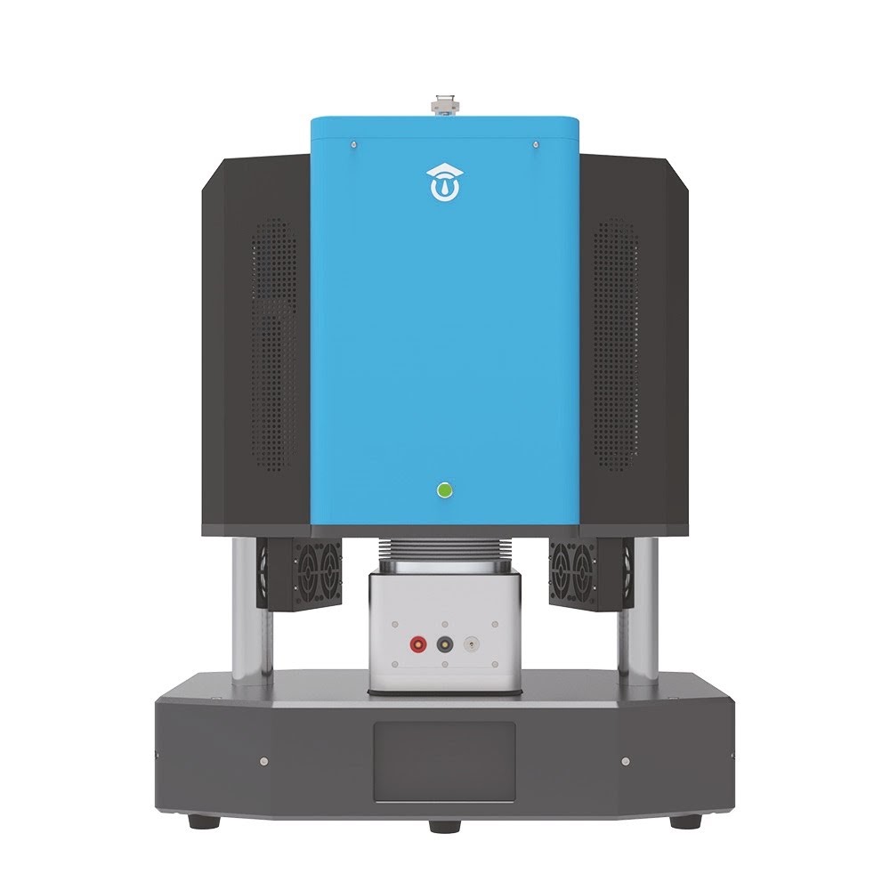
To execute reproducible volume resistivity and high-resistance insulation characterization on ceramic substrates across their full operational temperature envelope, the MatMeas HTS-1000HR High Temperature High Resistance Measurement System provides a specialized, automated metrology platform.
Operating across a temperature span from room temperature up to 1000°C under programmable PID heating rates, the HTS-1000HR features a triaxial guarded electrode fixture fabricated from high-purity sintered alumina pushrods and spring-loaded platinum contacts. The triaxial guarding topology routes surface leakage currents and furnace heating element hum directly to instrument ground, enabling measurement of ultra-high insulation resistances up to 10¹⁴ Ω with picoampere resolution (±1% accuracy from 100 kΩ to 10 TΩ). The integrated software automatically calculates temperature-dependent volume resistivity ρv, constructs Arrhenius plots, and extracts activation energies Ea in strict compliance with ASTM D1829.
Frequently Asked Questions
Why does 96% alumina experience an exponential loss of insulation resistance at temperatures above 300°C?
Commercial 96% alumina is fabricated with 4 wt% of silicate sintering aids (SiO2, CaO, MgO) to facilitate liquid-phase densification at lower sintering temperatures. Upon cooling, these additives form a continuous, amorphous aluminosilicate glass network along the crystalline Al2O3 grain boundaries. While stable at room temperature, temperatures above 300°C thermally mobilize alkali (Na⁺, K⁺) and alkaline earth (Ca²⁺) ions within this glassy phase. Under applied DC electrical fields, these mobile ions drift along grain boundaries, generating significant ionic leakage current that reduces volume resistivity by orders of magnitude.
How does surface roughness (Ra) affect electrical reliability in power electronic substrates?
Surface micro-roughness creates two distinct reliability hazards. First, microscopic asperities and peaks act as sharp electrostatic stress concentrators, locally amplifying electric fields and initiating partial discharges or premature dielectric breakdown. Second, when applying thin-film metallization (sputtered Ti/Cu or Ni/Au), high surface roughness (Ra > 0.3 μm) creates shadowing defects, step-coverage discontinuities, and localized stress concentrations that promote metallization blistering and delamination during thermal power cycling. High-purity 99.6% alumina offers an as-fired Ra < 0.1 μm, ensuring uniform field distribution and robust metallization adhesion.
What is the advantage of using a three-terminal guarded electrode fixture in ASTM D257 testing?
In two-terminal resistance measurements of thin ceramic substrates, electric current splits into two parallel paths: bulk volume current flowing through the thickness of the ceramic, and surface leakage current flowing across the outer perimeter of the sample (driven by adsorbed moisture or surface contamination). Because surface resistance is often much lower than bulk resistance, a two-terminal measurement records a combination of both paths, severely underestimating the true volume resistivity. A three-terminal guarded electrode surrounds the central measurement electrode with an annular guard ring held at the same potential, diverting surface leakage current directly to ground and ensuring that the ammeter measures only pure bulk volume current.
Request High-Precision Testing Solutions
Get expert guidance and customized instruments for your functional materials project.