Ceramic Substrate Dielectric Permittivity Evaluation
Technical News
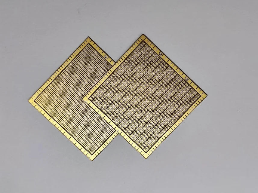
In advanced semiconductor modules, automotive power traction inverters, and 5G telecommunication hardware, ceramic substrates serve as critical structural platforms for semiconductor dies. Polycrystalline technical ceramics, including alumina (Al2O3), aluminum nitride (AlN), and silicon nitride (Si3N4), provide indispensable mechanical stiffness, electrical isolation, and thermal dissipation under rigorous working environments.
Among the foundational functional properties of these materials, dielectric permittivity (relative dielectric constant, ε') and dielectric loss tangent (tan delta) represent decisive physical metrics. These electromagnetic parameters dictate signal propagation velocity, capacitive crosstalk, parasitic phase delays, and localized power dissipation across high-density electronic assemblies. Rigorous dielectric characterization throughout engineering development and volume manufacturing provides essential data to stabilize product quality.
The Critical Role of Dielectric Properties in Ceramic Packaging
Miniaturization and elevated switching frequencies across modern electronic systems make circuit performance increasingly sensitive to substrate dielectric characteristics:
-
High-Speed Signal Transmission and Latency Reduction: In microwave antennas, millimetre-wave radar sensors, and 5G wireless front-end modules, signal propagation delay is proportional to the square root of the dielectric constant. Substrates exhibiting low and uniform permittivity mitigate electromagnetic dispersion, preserving digital pulse integrity and minimizing transmission loss.
-
Electrical Isolation and Voltage Endurance: In high-power semiconductor packages, such as silicon carbide (SiC) and gallium nitride (GaN) motor drives, substrate materials encounter electric field stresses exceeding several kilovolts per millimeter. Inconsistent permittivity distributions induce localized electric field distortions, escalating internal partial discharge activity and accelerating dielectric breakdown.
-
Thermal Management and Energy Efficiency: Dielectric loss represents the proportion of electromagnetic energy converted into heat within the insulating lattice. In high-power radio-frequency circuits, elevated loss tangents produce parasitic dielectric heating, compounding thermal burdens on adjacent semiconductor dies and diminishing overall module efficiency.
Key Factors Governing Substrate Dielectric Performance
The dielectric response of technical ceramic substrates is governed by intrinsic crystalline features, microstructural morphology, and operational testing parameters:
-
Purity and Secondary Intergranular Phases: Sintering aids (such as calcia, silica, or magnesia) form glassy intergranular phases at grain boundaries. Under alternating electric fields, mobile impurity ions within these boundary zones exhibit interfacial polarization, driving up dielectric loss.
-
Porosity and Microstructural Density: Residual microporosity substantially alters effective permittivity. Because air possesses a relative permittivity near 1.0, unclosed voids lower nominal dielectric constants while acting as high-stress concentration sites that compromise breakdown strength.
-
Frequency Dispersion: Dielectric polarization mechanisms vary markedly with operating frequency. While ionic and electronic displacements respond at gigahertz frequencies, dipolar and space-charge polarizations relax at lower kilohertz ranges, generating characteristic dielectric dispersion profiles.
-
Thermal Coefficients of Permittivity: Elevated operating temperatures alter atomic lattice spacing and increase charge carrier mobility, leading to positive temperature coefficients of capacitance. Substrates in automotive under-hood inverters must maintain stable permittivity across severe thermal transitions.
Metrological Challenges Across Temperature and Frequency Domains
Accurately measuring the dielectric constant and loss tangent of thin, highly insulating ceramic substrates introduces considerable metrological complexity:
-
Electrode-Sample Interface Contacts: Incomplete physical contact between rigid measurement electrodes and ceramic surfaces produces microscopic air gaps. These air gaps introduce parasitic series capacitances, resulting in underreported true dielectric constant values unless guarded thin-film gold or platinum metallization is deposited.
-
High-Temperature Fixture Leakage: Heating test fixtures to several hundred degrees Celsius induces parasitic conductance along support insulators. Guarded three-terminal topologies and shielded transmission fixtures are essential to shunt stray surface currents away from sensitive electrometer circuits.
-
Dynamic Atmospheric Influences: Atmospheric moisture adsorbs rapidly onto porous or micro-rough ceramic faces, inducing erroneous dielectric loss peaks at low frequencies. Stable characterization requires environmentally sealed measurement chambers capable of vacuum evacuation or dry inert gas purging.
Precision Dielectric Characterization with the MatMeas DMS1000
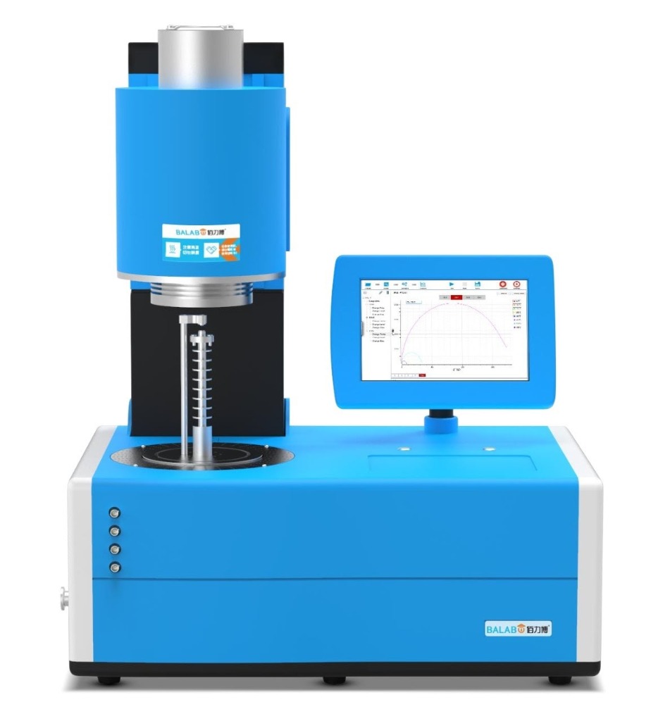
To overcome these metrological hurdles and deliver reproducible material parameters, the MatMeas DMS1000 provides a dedicated high-temperature dielectric impedance characterization system.
The DMS1000 system is engineered to evaluate bulk materials and technical ceramic substrates from room temperature up to 1000°C. With a broad frequency coverage spanning 20 Hz to 30 MHz and a measurement accuracy of 0.05%, the instrument resolves fine variations in capacitance, impedance, and loss tangent across multiple decades of excitation frequency.
Featuring an integrated sealable metal shielding enclosure, high-purity platinum electrodes, and programmable PID thermal control stable within ±0.5°C, the DMS1000 supports measurements under inert, oxidizing, reducing, and vacuum environments. Its sample holder architecture ensures consistent mechanical contact pressure without micro-cracking fragile ceramic plates. By delivering precise permittivity-temperature and impedance spectra, the platform enables research laboratories and substrate manufacturers to refine sintering formulations, establish rigorous quality thresholds, and ensure reliable electronic packaging.
Frequently Asked Questions
Why does dielectric loss tangent (tan delta) rise sharply at elevated temperatures in ceramic substrates?
At elevated temperatures, thermal excitation provides sufficient energy for bound ionic charges and intrinsic defect dipoles to overcome lattice potential barriers. Their intensified hopping conduction and interfacial polarization under alternating electric fields dissipate additional electromagnetic energy as heat, causing the dielectric loss tangent to rise by orders of magnitude.
How does substrate permittivity variation affect high-frequency RF impedance matching?
Microstrip transmission line characteristic impedance depends inversely on the square root of substrate dielectric permittivity. If permittivity fluctuates across a ceramic production batch, characteristic impedance deviates from designed target values (such as 50 ohms). This mismatch generates signal reflections, increased standing wave ratios, and phase distortion in high-frequency communication circuits.
Request High-Precision Testing Solutions
Get expert guidance and customized instruments for your functional materials project.