Ceramic Substrate Dielectric Loss Testing: Principles and Analysis
Technical News
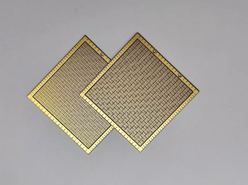
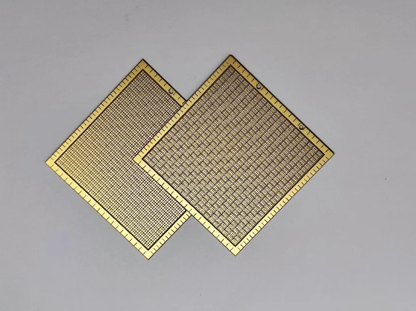
Ceramic substrates serve as critical electrical insulation and structural platforms in radio frequency (RF) communications, millimeter-wave radar systems, and high-density power semiconductor modules. In high-frequency and high-voltage operational regimes, passive material performance is governed not only by mechanical stiffness and thermal conductivity, but fundamentally by electrical energy dissipation under alternating electric fields. Dielectric loss testing quantifies this electrodynamic dissipation, providing essential data to predict electromagnetic signal attenuation, prevent internal thermal runaway, and ensure operational reliability across demanding thermal and frequency domains.
Evaluating the dielectric loss tangent (tan δ) alongside real permittivity enables microwave and power electronics engineers to validate incoming substrate lots against strict loss budgets, refine sintering formulations, and establish safe thermal envelopes for high-density multi-chip modules.
Mechanics and Mathematical Formulation of Dielectric Loss
When an alternating electric field traverses an insulating ceramic substrate, internal bound charges displace in an attempt to synchronize with the oscillating field. Because microscopic charge displacement is constrained by lattice inertia, viscous intergranular friction, and defect trapping, a phase lag (δ) develops between the applied electric field and the resulting displacement current.
In electrodynamics, this behavior is formulated using complex relative permittivity:
ε* = ε' - j * ε''
where ε' is real relative permittivity (quantifying capacitive energy storage, evaluated via ceramic substrate dielectric constant testing) and ε'' is the imaginary dielectric loss factor (quantifying irreversible dissipation into heat). The dielectric loss tangent is defined as the ratio:
tan δ = ε'' / ε'
The total loss tangent reflects three distinct physical transport and relaxation mechanisms:
tan δ = [ σ_dc / ( ω * ε_0 * ε' ) ] + [ ε_dipolar'' / ε' ] + [ ε_interfacial'' / ε' ]
where σ_dc is DC volume conductivity, ω = 2 * π * f is angular frequency, ε_0 is vacuum permittivity, and the remaining terms represent dipolar relaxation and Maxwell-Wagner interfacial polarization.
Under alternating electric fields, the volumetric power dissipated as heat (P_d) within the ceramic core scales directly with the loss tangent:
P_d = ω * E^2 * ε_0 * ε' * tan δ (W/m^3)
In high-power RF transmitters and automotive motor inverters, elevated tan δ values induce severe self-heating, which can compound thermal stresses and trigger thermal breakdown.
Benchmark of Dielectric Loss Tangent Across Ceramic Substrates
Substrate materials exhibit distinct dielectric loss profiles across the frequency spectrum from kilohertz to gigahertz regimes.
| Substrate Formulation | Material Grade / Description | tan δ (1 kHz) | tan δ (1 MHz) | tan δ (10 MHz) | tan δ (10 GHz) | Dominant Loss Mechanism at 10 GHz | Typical RF Attenuation (dB/cm at 10 GHz) |
|---|---|---|---|---|---|---|---|
| 96% Al2O3 | Standard Electronic Substrate | 0.0020 - 0.0040 | 0.0010 - 0.0018 | 0.0012 - 0.0020 | 0.0015 - 0.0025 | Intergranular glassy silicate phase relaxation | 0.15 - 0.22 |
| 99.9% Al2O3 | Laser Thin-Film Grade | 0.0003 - 0.0006 | 0.0001 - 0.0002 | 0.0001 - 0.0003 | 0.0001 - 0.0004 | Intrinsic lattice phonon damping | 0.02 - 0.05 |
| AlN (Aluminum Nitride) | High Thermal Conductivity | 0.0010 - 0.0025 | 0.0005 - 0.0010 | 0.0005 - 0.0012 | 0.0008 - 0.0015 | Oxygen impurity substitution on nitrogen sites | 0.08 - 0.12 |
| Si3N4 (Silicon Nitride) | Active Metal Brazing (AMB) | 0.0040 - 0.0080 | 0.0025 - 0.0045 | 0.0025 - 0.0040 | 0.0030 - 0.0050 | Amorphous oxynitride grain boundary phase | 0.25 - 0.35 |
| LTCC Glass-Ceramic | High-Frequency Formulations | 0.0025 - 0.0050 | 0.0015 - 0.0025 | 0.0015 - 0.0028 | 0.0015 - 0.0030 | Borosilicate network relaxation | 0.12 - 0.20 |
| Fused Silica (SiO2) | Optical / Millimeter-Wave | 0.0001 - 0.0002 | < 0.0001 | < 0.0001 | 0.0001 - 0.0002 | Ultra-low intrinsic network damping | < 0.01 |
High-purity 99.9% alumina and fused silica provide the lowest dielectric loss at microwave frequencies, making them the preferred choices for low-loss stripline filters and millimeter-wave phased arrays.
Microscopic Dielectric Loss Mechanisms Across Frequency and Temperature
Dielectric dissipation in technical ceramics originates from four discrete physical mechanisms operating across distinct frequency domains and thermal envelopes:
| Dielectric Loss Mechanism | Physical Origin and Transport Kinetics | Characteristic Frequency Domain | Temperature Dependence | Experimental Diagnostic Signature |
|---|---|---|---|---|
| DC Conduction Loss | Drift of thermally activated free ions (alkali impurities, oxygen vacancies) | Low frequencies (< 100 kHz) | Increases exponentially with temperature (σ ~ exp(-E_a/kT)) | tan δ scales inversely with frequency (tan δ ~ 1/ω); no loss peak |
| Dipolar Debye Relaxation | Reorientation of localized defect dipoles (e.g., acceptor-oxygen vacancy pairs) | 100 kHz to 30 MHz | Relaxation peak shifts to higher frequencies with rising temperature | Characteristic bell-shaped tan δ peak governed by Arrhenius activation |
| Maxwell-Wagner Interfacial Loss | Charge carrier trapping at grain boundaries, phase interfaces, and micro-pores | 10 Hz to 100 kHz | Pronounced at intermediate-to-high temperatures (> 200°C) | Giant apparent permittivity at low frequencies accompanied by broad tan δ plateau |
| Intrinsic Phonon Damping | Interaction between electromagnetic waves and fundamental optic lattice phonons | Microwave to THz (> 1 GHz) | Weak temperature dependence (scales linearly with temperature) | Loss factor increases linearly with frequency (ε'' ~ f); sets lower physical loss limit |
The classical Debye relaxation equations describe the frequency dependence of dipolar losses:
ε'(ω) = ε_inf + ( ε_s - ε_inf ) / ( 1 + ω^2 * τ^2 )
ε''(ω) = ( ε_s - ε_inf ) * ω * τ / ( 1 + ω^2 * τ^2 )
where ε_s is static low-frequency permittivity, ε_inf is high-frequency permittivity, and τ is relaxation time. A maximum in dielectric loss occurs at ω * τ = 1.
High-Frequency Signal Integrity and RF Attenuation
In RF communication hardware, 5G base stations, and automotive radar front-ends, dielectric loss within the substrate directly dictates transmission attenuation along microstrip and coplanar interconnects. The total attenuation constant (α_total) along a planar microstrip line combines conductor loss (α_c) and dielectric loss (α_d):
α_total = α_c + α_d
α_d = [ π * ε_r * ( ε_eff - 1 ) / ( ε_eff * ( ε_r - 1 ) ) ] * [ ( tan δ ) / λ_0 ] (Np/m)
where ε_eff is effective relative permittivity and λ_0 is free-space wavelength. At millimeter-wave frequencies (such as 28 GHz or 77 GHz), dielectric loss becomes the dominant contributor to signal attenuation, severely degrading transmission distance, antenna radiation efficiency, and receiver noise figure.
Microstructural Quality Screening via Loss Spectroscopy
Because dielectric loss is exceptionally sensitive to localized lattice imperfections, broadband dielectric spectroscopy—complemented by ceramic substrate impedance testing and high-temperature broadband dielectric testing for ceramic substrates—serves as a powerful non-destructive quality control method:
- Detection of Intergranular Silicate Phases: In alumina ceramics, even 1% to 4% glassy fluxing aids (SiO2, CaO, MgO) elevate tan δ at 1 MHz by more than an order of magnitude compared to pure alpha-alumina, revealing sub-standard raw powders.
- Identification of Sintering Pores and Microcracks: Trapped air voids induce localized Maxwell-Wagner interfacial charge accumulation, elevating low-frequency tan δ and signaling incomplete sintering densification.
- Oxygen Vacancy and Non-Stoichiometry Tracking: In functional ceramics, oxygen deficiency from reducing sintering atmospheres elevates ionic conduction losses, which appear as steep low-frequency loss tails.
High-Temperature Dielectric Characterization with MatMeas DMS-1000
Evaluating dielectric loss across wide temperature and frequency boundaries requires dedicated, highly stable metrology equipment.
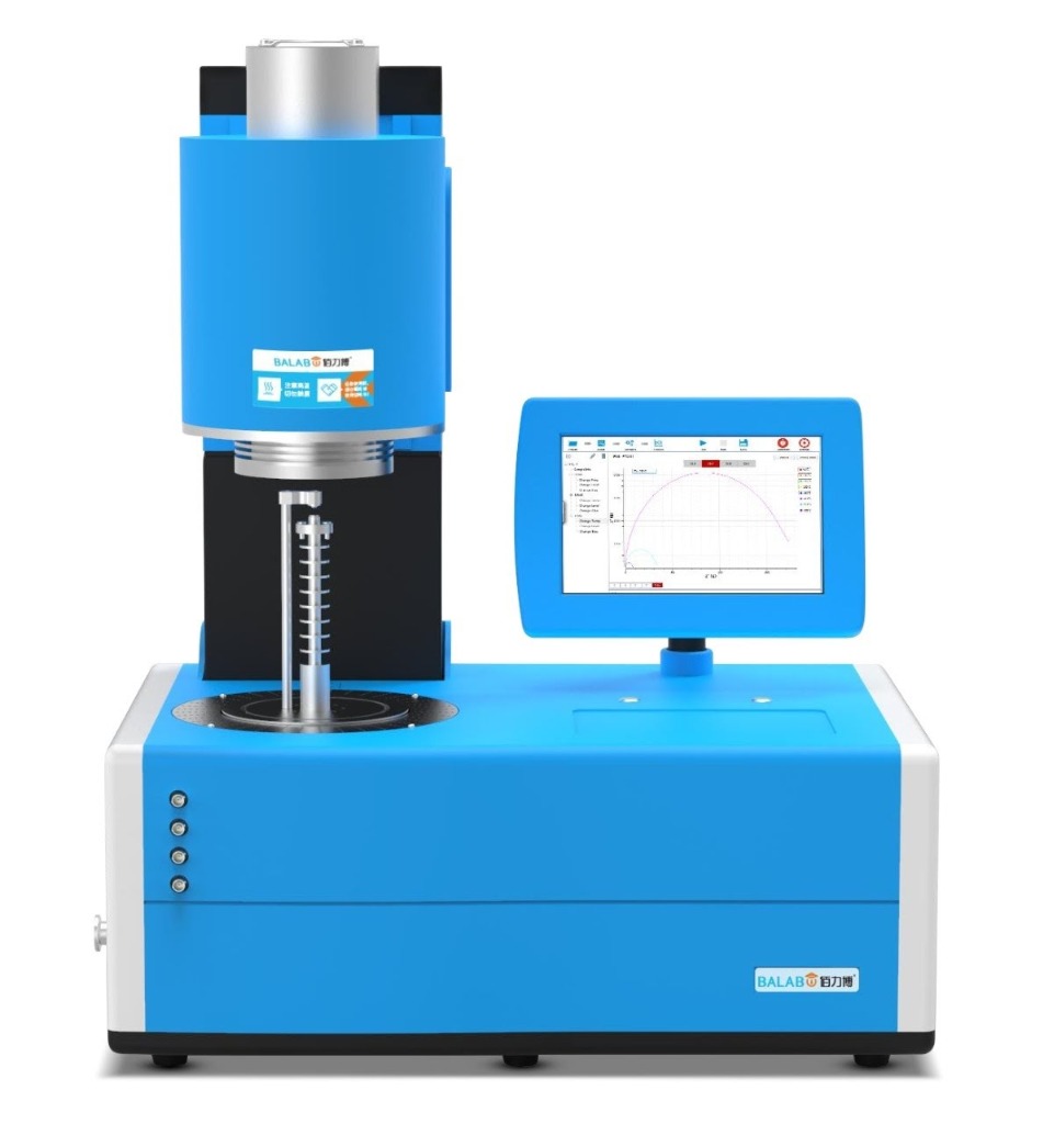
The MatMeas DMS-1000 high-temperature dielectric measurement system provides advanced impedance and dielectric loss characterization tailored for technical ceramics, substrates, and functional electronic materials.
Key technical specifications of the DMS-1000 include:
- Wide Thermal Operating Range (Ambient to 1000°C): Sealed high-temperature furnace with digital PID control maintains ±0.5°C thermal stability across multi-hour sweeps.
- Broad Frequency Bandwidth (20 Hz to 30 MHz): High-resolution impedance testing resolves minute dielectric loss tangents down to 0.0001 across multiple frequency decades.
- Multi-Atmosphere Testing Chamber: Supports measurements under vacuum, ambient air, inert gas (nitrogen, argon), and reducing atmospheres, preventing electrode oxidation and moisture artifacts.
- Guarded Platinum Electrode Fixtures: High-purity platinum electrodes with calibrated spring-loaded contacts ensure stable, non-oxidizing electrical interfaces up to 1000°C.
- Specimen Versatility: Accommodates ceramic discs, thick plates, and substrate coupons up to 20 mm in diameter and 5 mm thickness with automated parameter extraction.
Frequently Asked Questions
Why does dielectric loss in ceramic substrates increase rapidly at elevated temperatures?
At elevated temperatures, thermal agitation supplies kinetic energy that frees trapped charge carriers and accelerates the mobility of mobile ions and oxygen vacancies across grain boundaries. These mobile carriers contribute to DC electrical conduction and space-charge interfacial relaxation, increasing low-frequency dielectric loss (tan δ). The MatMeas DMS-1000 monitors this thermal activation from room temperature up to 1000°C with ±0.5°C control accuracy.
How does substrate dielectric loss directly degrade high-frequency RF circuits?
In RF and microwave circuits, dielectric loss converts electromagnetic signal energy directly into thermal heat within the substrate core. Higher tan δ increases transmission line attenuation, degrades the quality factor (Q) of resonators and planar bandpass filters, reduces antenna radiation efficiency, and introduces phase distortion across broadband signals.
What electrode configuration is recommended for high-temperature dielectric loss testing?
Base-metal electrodes (such as copper or silver paste) oxidize rapidly above 400°C in air, forming resistive oxide layers that introduce false series resistance and distort low loss tangent readings. High-temperature testing mandates noble metal electrodes. The MatMeas DMS-1000 utilizes high-purity platinum electrodes with calibrated spring-loaded fixtures to maintain uniform contact pressure and eliminate interface oxidation up to 1000°C.
Request High-Precision Testing Solutions
Get expert guidance and customized instruments for your functional materials project.