Ceramic Substrate Dielectric Spectrum Testing
Technical News
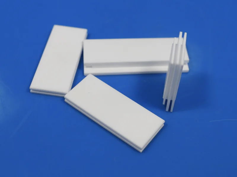
High-performance ceramic substrates—predominantly high-purity alumina (Al2O3), aluminum nitride (AlN), silicon nitride (Si3N4), and low-temperature co-fired ceramics (LTCC)—form the structural and electrical backbone of modern RF power amplifiers, 5G/6G millimeter-wave radar modules, and high-voltage power electronics (IGBT/SiC traction inverters). In high-frequency microstrip architectures, the relative dielectric permittivity (εr) and dielectric dissipation factor (loss tangent, tan δ) of the ceramic substrate directly dictate characteristic transmission line impedance, phase velocity, electromagnetic signal attenuation, and parasitic cross-talk.
Broadband dielectric spectroscopy (BDS) across a wide frequency range (100 Hz to 10 MHz) and temperature spectrum (−150°C to 1000°C) is essential to map the fundamental dielectric response of substrates. At elevated temperatures or high operational frequencies, secondary intergranular glassy phases, alkali metal impurities, and trapped oxygen vacancies induce severe Maxwell-Wagner interfacial polarization. These defect mechanisms cause sudden upturns in dielectric loss that degrade high-frequency microwave transmission lines. Characterizing these dielectric phenomena requires rigorous metrology conforming to international standards.
Fundamental Physics of Complex Permittivity and Loss Mechanisms
Dielectric behavior under an alternating electric field is defined by the complex relative permittivity ε*( ω):
ε*( ω) = ε′( ω) − j · ε″( ω)
where ε′ represents the real relative permittivity (dielectric constant), quantifying the reversible energy storage capacity through unit-cell polarization, and ε″ is the imaginary dielectric loss factor, representing irreversible energy dissipation as heat. The dielectric dissipation factor, or loss tangent, is defined as the ratio:
tan δ = ε″ / ε′ = 1 / (ω · Rp · Cp)
where ω = 2 · π · f is the angular frequency, and Rp and Cp are the equivalent parallel resistance and capacitance of the substrate specimen under parallel-plate test geometry.
Total dielectric loss in polycrystalline ceramic substrates arises from four distinct physical mechanisms:
tan δtotal = tan δintrinsic + tan δdipole + tan δMW + tan δconduction
-
Intrinsic Lattice Phonon Absorption (tan δintrinsic): Anharmonic interactions between the external electromagnetic wave and fundamental crystal lattice phonons (dominant in microwave bands above 1 GHz).
-
Impurity Defect Dipole Relaxation (tan δdipole): Thermally activated reorientation of point-defect complexes (e.g., divalent metal impurities paired with oxygen vacancies).
-
Maxwell-Wagner Interfacial Polarization (tan δMW): Charge carrier accumulation at heterogeneous phase boundaries between highly insulating crystalline grains and semi-conductive amorphous grain boundary glassy phases.
-
DC Leakage Conduction (tan δconduction): Ohmic loss resulting from long-range migration of free electrons or mobile ions:
tan δconduction = σdc / (ω · ε0 · ε′)
Notice that σdc causes tan δ to rise steeply as frequency ω decreases toward low frequencies (f < 1 kHz) or as temperature rises.
Comprehensive Benchmark of Electronic and Power Ceramic Substrates
Substrate selection requires balancing dielectric permittivity, dielectric loss, thermal conductivity, and mechanical fracture toughness.
The comprehensive benchmark table below details the dielectric and thermomechanical properties of the primary engineering ceramic substrates:
| Ceramic Substrate Material | Dominant Chemical Composition | Relative Permittivity ε′ (1 MHz, 25°C) | Dissipation Factor tan δ (1 MHz, 25°C) | High-Frequency tan δ (10 GHz, 25°C) | Thermal Conductivity κ (W/m·K) | Dielectric Strength Eb (kV/mm) | Primary Application Focus |
|---|---|---|---|---|---|---|---|
| 96% Alumina (Al2O3) | Al2O3 + 4% SiO2-CaO-MgO glass | 9.0–9.4 | 3.0–6.0 × 10⁻⁴ | 8.0–12.0 × 10⁻⁴ | 20–24 | 15–18 | General thick-film hybrid circuits, automotive sensors |
| 99.6% Alumina (Thin Film) | High-purity Al2O3 (<0.1% glass) | 9.8–10.0 | 0.8–1.5 × 10⁻⁴ | 1.5–3.0 × 10⁻⁴ | 30–35 | 20–25 | Microwave thin-film circuits, RF interconnects |
| Aluminum Nitride (AlN) | AlN + Y2O3 sintering aid | 8.6–8.9 | 3.0–7.0 × 10⁻⁴ | 5.0–10.0 × 10⁻⁴ | 170–200 | 18–22 | High-power SiC/GaN power modules, laser diodes |
| Silicon Nitride (Si3N4) | Si3N4 + rare earth oxides | 8.1–8.5 | 8.0–15.0 × 10⁻⁴ | 12.0–20.0 × 10⁻⁴ | 80–90 | 25–30 | EV traction inverters, high-toughness AMB substrates |
| LTCC (Low Temp Co-fired) | Glass-ceramic composite (crystallized) | 5.8–7.5 | 10.0–25.0 × 10⁻⁴ | 15.0–35.0 × 10⁻⁴ | 3–5 | 12–15 | 3D multi-layer RF front-end modules, radar radar antennas |
International Standards and Test Fixture Geometry
Evaluating complex permittivity on substrate tiles must comply with standard test methods, specifically ASTM D150 (Standard Test Methods for AC Loss Characteristics and Permittivity of Solid Electrical Insulation), IEC 60250, and IPC-TM-650 (Method 2.5.5.1).
Under parallel-plate electrode geometry, the measured capacitance C relates to ε′ through the effective electrode area Aeff and substrate thickness d:
C = ε0 · ε′ · (Aeff / d)
To eliminate edge fringing field errors (Cfringing) that distort readings on thin substrate coupons, a three-terminal guarded electrode geometry is mandatory:
Aeff = π / 4 · (D1 + g)²
where D1 is the diameter of the central guarded measuring electrode and g is the radial guard gap width. The guard ring shunts edge fringing electric field lines directly to instrument ground, ensuring strictly uniform perpendicular field lines within the measured volume.
The table below outlines common dielectric spectroscopy measurement anomalies and their experimental resolutions:
| Observed Spectral Anomaly | Underlying Physical / Experimental Artifact | Affected Frequency / Temp Range | Hardware & Procedural Mitigation Strategy |
|---|---|---|---|
| Low-Frequency Capacitance Upturn | Electrode polarization / air-gap series capacitance | f < 100 Hz, ambient or elevated temp | Apply sputtered thin-film gold electrodes; tighten spring-loaded probe force |
| Sharp Dielectric Loss Spike near 100°C | Desorption of physisorbed water moisture in micro-pores | 80°C to 120°C during initial ramp | Enforce 120°C vacuum bake-out for 1 hour prior to acquiring baseline |
| Massive High-Temp tan δ Tail | DC ionic hopping conduction (σdc / ω) | T > 500°C across low-to-mid frequencies | Extract AC conductivity using complex impedance Z″ deconvolution |
| High-Frequency Inductive Zero-Crossing | Lead wire residual inductance (Lresidual) resonance | f > 1 MHz on long furnace cables | Execute open/short/load impedance compensation at fixture terminals |
Advanced High-Temperature Metrology: MatMeas DMS-1000 System
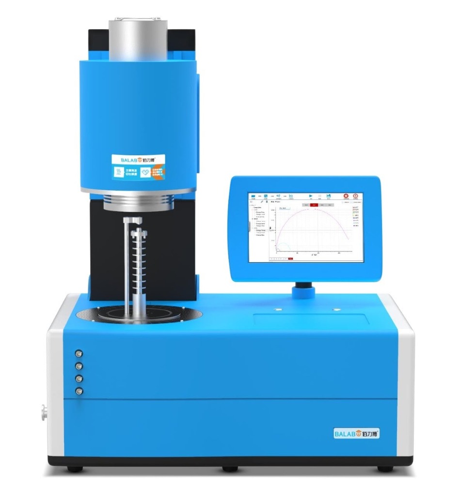
Characterizing advanced ceramic substrates across aggressive automotive and aerospace operating envelopes requires instrumentation capable of tracking dielectric parameters under simultaneous thermal and frequency sweeps. The MatMeas DMS-1000 High Temperature Dielectric Spectrometer provides an automated characterization platform operating from room temperature up to 1000°C across frequencies from 10 μHz up to 30 MHz (expandable to microwave bands).
The DMS-1000 fixture features high-purity recrystallized alumina pushrods paired with platinum-rhodium electrodes and spring-loaded mechanical tensioners. This architecture maintains constant mechanical contact pressure (0.5 to 2.0 N) as the ceramic substrate undergoes thermal expansion, preventing air-gap delamination. Integrated triaxial guarding eliminates furnace heater noise and parasitic leakage current, enabling resolution of ultra-low dielectric loss tangents down to 1 × 10⁻⁴ even at elevated temperatures.
Frequently Asked Questions
Why does 99.6% alumina exhibit significantly lower dielectric loss than 96% alumina at high frequencies?
The primary difference lies in the grain boundary chemistry. Commercial 96% alumina incorporates approximately 4 wt% of silicate-based sintering aids (SiO2, CaO, MgO) to facilitate liquid-phase sintering at lower temperatures (~1500°C). This leaves an amorphous, glassy intergranular phase rich in mobile alkali and alkaline-earth ions. At frequencies above 1 MHz, these mobile ions oscillate, generating substantial Maxwell-Wagner interfacial relaxation loss. High-purity 99.6% alumina is sintered via solid-state diffusion, yielding clean, direct grain-to-grain contact with negligible glassy phase, which minimizes high-frequency dielectric loss.
How does parasitic air-gap capacitance alter the measured dielectric constant of thin substrate tiles?
If dry electrodes are simply clamped against a substrate without conductive metallization, microscopic surface roughness creates an unavoidable microscopic air gap in series with the ceramic. Because air has a much lower permittivity (εair = 1) than the ceramic (εceramic ≈ 9–10), the total capacitance of two series capacitors is dominated by the lower capacitance. This causes the instrument to severely underestimate the real permittivity of the substrate. Applying direct sputtered or evaporated gold electrodes eliminates this air layer, ensuring accurate measurement.
What causes dielectric loss tangent tan δ to rise exponentially at temperatures above 500°C?
At temperatures exceeding 500°C, intrinsic oxygen vacancies and defect electrons gain sufficient thermal energy to overcome hopping activation barriers (Ea), leading to high DC electrical conductivity (σdc). Because dielectric loss contains an ohmic term defined by tan δconduction = σdc / (ω · ε0 · ε′), an exponential increase in conductivity drives a corresponding exponential increase in measured loss, particularly at lower frequencies.
Request High-Precision Testing Solutions
Get expert guidance and customized instruments for your functional materials project.