Piezoelectric Thin Film Electrical Performance Testing
Technical News
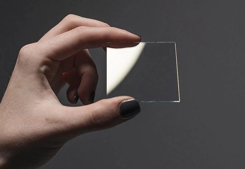
Piezoelectric thin films—primarily wurtzite aluminum nitride (AlN), scandium-doped aluminum nitride (ScxAl1-xN), sol-gel lead zirconate titanate (PZT), and ferroelectric polymer films such as P(VDF-TrFE)—are key functional components in modern RF acoustic filters (BAW/FBAR), micro-electro-mechanical systems (MEMS) micromirrors, piezoelectric micromachined ultrasonic transducers (PMUTs), and vibrational energy harvesters. Operating at sub-micron to several-micrometer thicknesses, these functional layers translate electrical signals into mechanical acoustic resonance with gigahertz frequency response.
However, characterizing the electrical and electromechanical properties of thin films introduces severe physical and experimental constraints that do not exist in bulk ceramics. The most fundamental constraint is two-dimensional mechanical substrate clamping: because the thin piezoelectric film is rigidly adhered to a massive underlying silicon or sapphire wafer, lateral strain is completely suppressed. Furthermore, sub-micron film thicknesses create massive internal electric fields under modest voltages, accelerating dielectric leakage current and phase-lag errors. Overcoming these characterization bottlenecks requires specialized metrology frameworks and substrate clamping corrections.
Substrate Clamping Mechanics and the Lefki-Dormans Constitutive Model
In bulk piezoelectric ceramics, application of an electric field along the polarization axis (E3) produces unconstrained longitudinal expansion (S3 = d33 · E3) accompanied by transverse Poisson contraction (S1 = S2 = d31 · E3). When the piezoelectric layer is integrated as a thin film onto a comparatively thick substrate (e.g., a 1 μm film on a 500 μm silicon wafer), the rigid substrate enforces a zero-in-plane strain boundary condition (S1 = S2 = 0).
Under this rigid clamping boundary condition, the transverse strain cannot relax freely, generating massive in-plane mechanical stresses (T1 = T2 ≠ 0). Through transverse piezoelectric coupling (d31), these in-plane stresses counteract the out-of-plane longitudinal displacement. The resulting effective, or clamped, longitudinal piezoelectric coefficient (d33,f) is derived using the classical Lefki-Dormans formulation:
d33,f = d33 − 2 · [s13E / (s11E + s12E)] · d31
where sijE are elastic compliance coefficients of the piezoelectric film under constant electric field. Because d31 and s13E are negative quantities in perovskites and wurtzites, the term 2 · [s13E / (s11E + s12E)] · d31 is positive, which substantially reduces the effective piezoelectric response. For standard PZT compositions, substrate clamping suppresses the observable longitudinal piezoelectric displacement by 40% to 60% compared to unconstrained bulk ceramics:
d33,f ≈ (0.4 to 0.6) · d33,bulk
Similarly, the effective transverse piezoelectric stress coefficient e31,f, which directly dictates PMUT membrane deflection and cantilever actuation, is defined as:
e31,f = d31 / (s11E + s12E) = e31 − [c13E / c33E] · e33
where cijE represent elastic stiffness constants. Accurate device modeling requires extracting both d33,f and e31,f while accounting for substrate stiffness.
Comprehensive Benchmark: Thin Film vs. Bulk Piezoelectric Systems
Different piezoelectric thin film formulations offer distinct trade-offs between electromechanical coupling, dielectric permittivity, breakdown field, and acoustic velocity.
The comparative matrix below details performance metrics across the leading piezoelectric thin film technologies compared to their bulk ceramic counterparts:
| Piezoelectric Film Material | Deposition Technique | Film Thickness Window (μm) | Effective Clamped d33,f (pC/N) | Effective Transverse e31,f (C/m²) | Relative Permittivity εr (100 kHz) | Dielectric Breakdown Field Eb (MV/m) | Primary Device Applications |
|---|---|---|---|---|---|---|---|
| Pure Aluminum Nitride (AlN) | Reactive magnetron sputtering | 0.5–2.0 | 4.0–5.5 | −0.95 to −1.15 | 9.0–10.5 | 300–450 | 5G BAW/FBAR filters, high-frequency resonators |
| Scandium AlN (Sc0.3Al0.7N) | Co-sputtering / alloy targets | 0.5–1.5 | 14.0–18.0 | −2.40 to −3.10 | 14.0–16.5 | 250–350 | Wideband 5G/6G RF filters, high-SNR PMUT arrays |
| Sol-Gel PZT (52/48 MPB) | Spin-coating / rapid thermal anneal | 0.5–4.0 | 60–120 | −8.0 to −14.0 | 800–1400 | 120–180 | MEMS inkjet printheads, LiDAR micromirrors |
| Epitaxial BTO (BaTiO3) | Pulsed laser deposition (PLD) | 0.1–0.5 | 30–50 | −3.0 to −5.5 | 300–600 | 150–220 | Lead-free optical modulators, non-volatile FeRAM |
| P(VDF-TrFE) Copolymer | Solvent spinning / thermal anneal | 0.2–2.0 | −18.0 to −25.0 | −1.5 to −2.2 | 8.5–11.0 | 180–260 | Flexible tactile sensors, wearable ultrasound |
International Standards and Metrology Protocols
Characterizing piezoelectric thin films requires strict adherence to international standards governing microelectronic and MEMS thin films, specifically IEEE Std 176 and SEMI MS4-0307 (Standard Guide for Measurement of Electrical Properties of Thin Films).
Standardized test procedures require:
- Top Electrode Lithographic Micro-Patterning: Continuous conductive films must be lithographically patterned into discrete circular micro-capacitors (dot diameters ranging from 50 μm to 500 μm). Testing across un-patterned continuous metallization leads to uncontrolled lateral fringing field capacitance and distributed current spreading.
- Bottom Ground Plane Access: Low-resistance ohmic contact to the buried bottom electrode (typically Pt/Ti or TiN/Al) must be established by selective chemical etching or mechanical ultrasonic micro-wire bonding.
- Leakage Current Decoupling: High leakage currents in thin films (Jleak > 10⁻⁴ A/cm²) introduce severe artificial phase shifts during small-signal capacitance testing. Cryogenic testing down to liquid nitrogen temperatures (−160°C) is effective in freezing thermally activated Poole-Frenkel or Schottky emission leakage, isolating the true intrinsic dielectric and electromechanical response.
The table below outlines common thin-film electrical artifacts and experimental remedies:
| Thin Film Testing Artifact | Root Physical Mechanism | Symptom in Data | Hardware / Procedural Mitigation |
|---|---|---|---|
| Banana-Shaped P-E Loops | High DC ohmic or lossy leakage conductance | Hysteresis loop tips fail to close; apparent Pr artificially elevated | Implement 5-pulse PUND testing; cool specimen to cryogenic temps |
| Bottom Electrode Contact Resistance | Oxidized adhesion layer (Ti/TiOx) or bad probe contact | Frequency dispersion in capacitance (C drops steeply at >100 kHz) | Perform 4-point micro-probing; use sputtered Au contact pads |
| Substrate Bending Parasitic | Global wafer curvature induced by cantilever deflection | Low-frequency d33,f inflated by wafer flexure mode | Restrict testing frequency to >1 kHz; clamp wafer to rigid vacuum chuck |
| Dielectric Breakdown at Dot Perimeter | Electric field concentration at sharp lithographic electrode edges | Abrupt irreversible short circuit at modest fields (<50 MV/m) | Deposit passivating SiO2 margin; taper electrode etching profile |
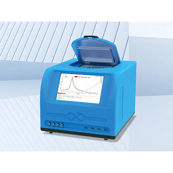
Advanced Thin Film Metrology: MatMeas DMS-2000 Cryogenic Platform
Characterizing thin films across wide temperature and frequency boundaries requires specialized low-noise instrumentation. The MatMeas DMS-2000 Low-Temperature Dielectric Spectrometer provides an integrated testing environment operating across temperatures from −160°C up to 300°C (with liquid nitrogen cooling) and frequencies from 10 μHz to 30 MHz.
The DMS-2000 integrates micro-manipulated coaxial Kelvin probes within an evacuated thermal test chamber, completely preventing ambient moisture condensation at sub-zero temperatures. High-precision capacitance bridges resolve ultra-low capacitance signals down to 10 fF on microscopic dots (100 μm diameter). By freezing out thermally activated defect hopping at cryogenic temperatures, the platform isolates intrinsic lattice dielectric properties, enabling accurate extraction of d33,f, dielectric loss tan δ, and ferroelectric switching dynamics.
Frequently Asked Questions
Why is the measured d33 of a PZT thin film significantly lower than that of bulk PZT ceramic?
The reduction in observable d33 is a direct consequence of two-dimensional mechanical substrate clamping. In bulk ceramics, the material expands longitudinally while contracting freely in the lateral directions (d31). In a thin film adhered to a thick silicon substrate, the substrate completely constrains lateral contraction (S1 = S2 = 0). This generates massive in-plane compressive stresses that, through transverse piezoelectric coupling, counteract out-of-plane longitudinal expansion. According to the Lefki-Dormans equation, this mechanical constraint suppresses the effective clamped coefficient d33,f by 40% to 60%.
How does Sc doping improve the piezoelectric performance of AlN thin films?
Pure wurtzite AlN exhibits an intrinsically modest piezoelectric response (d33 ≈ 5 pC/N) due to its rigid covalent wurtzite crystal structure. Substituting scandium (Sc³⁺) for aluminum (Al³⁺) on the cation sublattice introduces structural instability, softening the wurtzite lattice toward a metastable non-polar hexagonal phase. This lattice softening substantially increases elastic compliance (s33E) and enhances structural dipole displacement under stress, boosting d33 to over 15 to 18 pC/N at 30 mol% Sc while maintaining high acoustic velocity and low dielectric loss.
What causes "banana-shaped" polarization loops in ferroelectric thin films, and how are they avoided?
Banana-shaped P-E hysteresis loops occur when the thin film suffers from high DC electrical leakage current. Standard Sawyer-Tower or virtual-ground circuits integrate all charge flowing into the capacitor—both true ferroelectric domain switching charge and continuous ohmic conduction current. When leakage current is high, the accumulated charge Q = ∫ I dt creates open, rounded, artificial hysteresis loops. This artifact is eliminated by employing positive-up-negative-down (PUND) pulse testing to subtract non-switching leakage charge, or by cooling the specimen to cryogenic temperatures using liquid nitrogen to freeze out thermal leakage.
Request High-Precision Testing Solutions
Get expert guidance and customized instruments for your functional materials project.