High Frequency Ceramic Substrate Permittivity Testing for RF and Microwave Packaging
Technical News
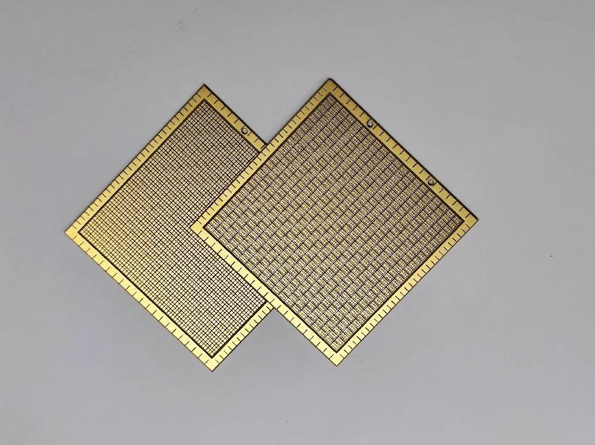
In modern high-speed microelectronics, millimeter-wave telecommunications, and power semiconductor packaging, executing accurate high frequency ceramic substrate permittivity testing is vital to ensuring signal integrity and impedance matching. As operational frequencies ascend into millimeter-wave radar bands (24 GHz to 77 GHz) and power densities surge in silicon carbide (SiC) and gallium nitride (GaN) modules, passive ceramic substrates must satisfy stringent electrodynamic and thermal dissipation criteria. Among all governing electrical properties, relative permittivity (dielectric constant, εr) dictates electromagnetic signal propagation velocity, characteristic transmission line impedance, capacitive crosstalk, and thermal dissipation. Rigorous permittivity testing is vital to ensure RF signal fidelity, suppress transmission reflections, and prevent high-temperature dielectric breakdown.
Selecting a ceramic substrate requires balancing mechanical rigidity, thermal conductivity, and dielectric permittivity. A mismatched or temperature-sensitive dielectric constant causes impedance discontinuities, reflection losses, and severe crosstalk in high-density multi-chip modules. Consequently, systematic permittivity characterization across realistic thermal and frequency spectrums represents a cornerstone of advanced packaging metrology.
Electrodynamic Role of Relative Permittivity in Ceramic Substrates
Relative permittivity measures a material's capability to polarize under an applied alternating electric field, storing electrostatic potential energy relative to a vacuum. In high-frequency microstrip, stripline, and coplanar waveguide architectures, substrate permittivity governs fundamental transmission physics:
- Phase Velocity and Propagation Delay: The phase velocity (
v_p) of an electromagnetic wave along a planar transmission line is inversely proportional to the square root of the effective relative permittivity (ε_eff):
v_p = c / sqrt( ε_eff )
t_pd = sqrt( ε_eff ) / c
where c is the speed of light in vacuum (3.0 * 10^8 m/s) and t_pd is the transmission propagation delay per unit length. Lower substrate permittivity yields higher signal velocities, directly minimizing transmission latency in high-speed digital interconnects and millimeter-wave phased-array feeds.
- Characteristic Impedance Matching: High-speed digital and RF traces require precisely controlled characteristic impedance (typically 50 Ω). For a standard microstrip line of trace width
won a substrate of thicknessh, characteristic impedanceZ_0is dictated by:
Z_0 = [ 87 / sqrt( ε_r + 1.41 ) ] * ln[ 5.98 * h / ( 0.8 * w + t_trace ) ]
Variations in substrate permittivity alter line capacitance per unit length, creating localized impedance steps that trigger signal reflection, standing waves, and elevated bit error rates.
- Capacitive Crosstalk and Package Miniaturization: In compact multi-layer packages, high dielectric constants promote parasitic capacitive coupling between adjacent signal lines, exacerbating signal crosstalk. Conversely, intermediate permittivity values facilitate structural miniaturization of stripline antennas and resonant filtering elements.
Benchmark of Electronic and Microwave Ceramic Substrates
Engineers must choose ceramic substrates tailored to specific thermal dissipation, dielectric constant, and loss tangent requirements across operating bands.
| Substrate Material | Purity / Dopant Class | Relative Permittivity εr (1 MHz) | Relative Permittivity εr (10 GHz) | Loss Tangent tan δ (10 GHz) | Thermal Conductivity k (W/m·K) | Coefficient of Thermal Expansion (ppm/K) | Primary Industry Application |
|---|---|---|---|---|---|---|---|
| 96% Al2O3 | Standard Electronic Grade | 9.4 - 9.8 | 9.2 - 9.5 | 0.0010 - 0.0020 | 20 - 24 | 6.8 - 7.2 | Thick-film circuits, automotive engine sensors, general packaging |
| 99.6% Al2O3 | Laser Thin-Film Grade | 9.8 - 10.0 | 9.7 - 9.9 | 0.0001 - 0.0004 | 28 - 32 | 7.0 - 7.4 | Thin-film RF microstrip circuits, microwave hybrid ICs |
| AlN (Aluminum Nitride) | High Thermal Purity | 8.6 - 9.0 | 8.5 - 8.8 | 0.0005 - 0.0010 | 170 - 200 | 4.5 - 4.7 | High-power SiC/GaN power modules, laser diode submounts |
| Si3N4 (Silicon Nitride) | High Toughness AMB | 8.1 - 8.4 | 8.0 - 8.3 | 0.0020 - 0.0040 | 80 - 90 | 3.0 - 3.2 | EV traction inverters, high-vibration power modules |
| LTCC (Glass-Ceramic) | Low-Temp Co-Fired | 5.8 - 7.5 | 5.6 - 7.2 | 0.0015 - 0.0030 | 3 - 5 | 5.5 - 6.5 | Multi-layer RF front-end modules, radar transceivers |
| Fused Silica (SiO2) | Optical / RF Grade | 3.8 - 3.9 | 3.8 - 3.85 | 0.0001 - 0.0002 | 1.4 - 1.6 | 0.5 - 0.6 | Millimeter-wave 77 GHz radar circuits, space communications |
Alumina provides robust mechanical rigidity and reliable dielectric stability. Aluminum nitride balances intermediate permittivity with exceptional thermal dissipation, while fused silica delivers the lowest dielectric constant and minimum insertion loss for ultra-high-frequency radar.
Frequency Dispersion and Dielectric Loss Mechanics
Substrate permittivity is fundamentally frequency-dependent, governed by electronic, ionic, dipolar, and interfacial (Maxwell-Wagner) polarization mechanisms. Across alternating electric fields, complex permittivity is expressed as:
ε* = ε' - j * ε''
tan δ = ε'' / ε'
where ε' is real relative permittivity (energy storage), ε'' is the imaginary loss factor (energy dissipation), and tan δ is the dielectric loss tangent. At radio frequencies (100 kHz to 30 MHz), space-charge and defect-dipole relaxations dominate. As excitation frequencies enter microwave bands (>1 GHz), dipolar relaxation peaks subside, leaving intrinsic ionic and lattice phonon damping as the primary loss mechanisms.
Sudden increases in dielectric loss across frequency bands indicate microstructural defects, unreacted fluxing phases, or mobile alkali ions within intergranular boundaries.
Methodological Comparison of Permittivity Measurement Techniques
Characterizing dielectric properties across wide frequency bands requires deploying distinct, complementary measurement topologies, as outlined in our comprehensive advanced ceramic substrate electrical testing guide. While low-to-mid frequency impedance spectroscopy evaluates temperature-dependent polarization mechanisms, microwave resonance methods measure ultra-low dielectric loss at specific carrier frequencies.
| Measurement Technique | Governing Standard | Frequency Coverage | Typical Permittivity Uncertainty | Loss Tangent Resolution | Thermal Sweep Feasibility | Specimen Preparation Requirements |
|---|---|---|---|---|---|---|
| Parallel-Plate Capacitance | ASTM D150 / IEC 60250 | 20 Hz to 30 MHz | ±0.5% to ±1.0% | 1.0 * 10^-4 | Excellent (-160°C to 1000°C) | Flat discs/squares; sputtered or painted parallel electrodes (see dielectric constant testing guide) |
| Split-Post Dielectric Resonator (SPDR) | IEC 61189-2-721 | 1 GHz to 20 GHz (Fixed) | ±0.5% to ±1.5% | 2.0 * 10^-5 | Limited (ambient to 85°C) | Thin planar sheets; non-metallized, no electrodes required |
| Resonant Cavity Perturbation | ASTM D2520 | 1 GHz to 35 GHz (Discrete) | ±1.0% to ±2.0% | 1.0 * 10^-4 | Moderate (-50°C to 300°C) | Precision rectangular rod or capillary coupon |
| Open-Ended Coaxial Probe | IEEE Std 1502 | 500 MHz to 50 GHz | ±3.0% to ±5.0% | 5.0 * 10^-3 | Poor (calibrated at 25°C) | Thick polished flat block; requires intimate probe contact |
Parallel-plate impedance spectroscopy represents the gold standard for continuous wideband frequency sweeps and wide-temperature profiling. It enables materials scientists to identify defect relaxation peaks, determine activation energies, and quantify thermal stability before fabricating high-frequency microwave resonators.
Temperature-Dependent Permittivity and Thermal Drift Analysis
Electronic assemblies operate across severe thermal excursions, from cryogenic space deployments (-150°C) to automotive engine compartments (150°C) and downhole geothermal probes exceeding 300°C. As temperature rises, volumetric lattice expansion tends to lower permittivity by diluting polarizable atoms per unit volume, while enhanced ionic polarizability acts in the opposite direction.
The net thermal drift is quantified by the Temperature Coefficient of Permittivity (TCε):
TCε = ( 1 / ε_ref ) * ( dε / dT ) * 10^6 (ppm/K)
In narrow-band microwave cavity filters and antenna arrays, uncontrolled TCε causes center-frequency thermal detuning:
Δf / f_0 = -0.5 * ( TCε + α_L ) * ΔT
where α_L is the substrate's linear coefficient of thermal expansion. Evaluating TCε over the intended operational temperature envelope is essential to design temperature-compensated dielectric systems.
Precision Dielectric Characterization with the MatMeas DMS-1000
Evaluating dielectric constant dispersion, phase transitions, and thermal drift requires specialized instrumentation capable of combining broad frequency sweeps with precision environmental temperature control.
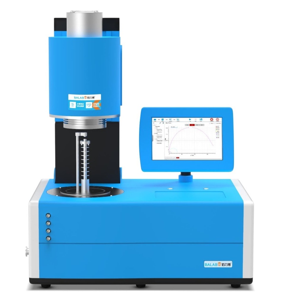
The MatMeas DMS-1000 temperature-dependent dielectric measurement system provides automated impedance and permittivity characterization across extreme thermal profiles. Operating over a continuous temperature span from ambient up to 1000°C (with available cryogenic liquid nitrogen options down to -160°C), the system pairs with high-precision impedance analyzers to cover frequencies from 10 μHz up to 30 MHz.
Equipped with sealed environmental chamber options for vacuum, inert gas, or oxidizing atmospheres, the DMS-1000 eliminates moisture condensation artifacts and prevents electrode oxidation. High-purity platinum electrodes and triaxial guarded shielding ensure that measured capacitance reflects pure material response, resolving dielectric loss tangents down to 0.0001. This wide-range capability enables engineers to evaluate low-to-mid frequency dielectric dispersion, track temperature coefficients, and verify material quality prior to final microwave device packaging.
Frequently Asked Questions
Why is low dielectric permittivity critical for millimeter-wave communication substrates?
Lower relative permittivity increases the phase velocity of electromagnetic waves along planar transmission lines, minimizing propagation latency. Additionally, lower permittivity reduces parasitic inter-trace capacitance, mitigating capacitive crosstalk and preserving signal integrity across high-density millimeter-wave packaging.
What is the primary operational difference between parallel-plate testing and split-post dielectric resonator (SPDR) testing?
Parallel-plate testing uses contact electrodes to sweep continuous frequencies from millihertz up to 30 MHz across wide temperature ranges (-160°C to 1000°C), ideal for mapping defect relaxation and temperature coefficients. SPDR testing operates at discrete microwave frequencies (such as 5 GHz or 10 GHz) without requiring electrodes, providing ultra-high sensitivity for loss tangent measurements at fixed temperatures.
How does ceramic porosity degrade high-frequency dielectric performance?
Pores inside sintered ceramics trap air, which has a dielectric constant near 1.0, lowering bulk permittivity in an uncontrolled manner. More critically, open pores readily absorb ambient moisture, which has a very high permittivity (~80) and high dielectric dissipation, leading to severe signal attenuation and thermal instability during device operation.
Request High-Precision Testing Solutions
Get expert guidance and customized instruments for your functional materials project.