Ceramic Substrate Silvering: Process Selection Guide
Technical News
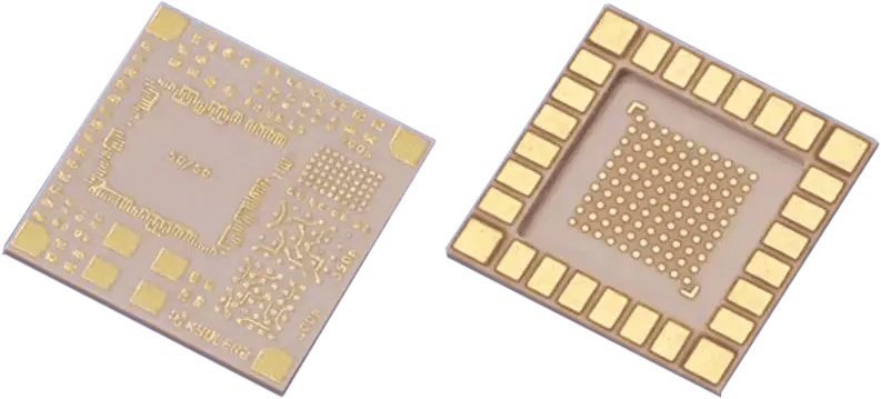
Ceramic substrates, particularly alumina and aluminum nitride, are vital in power electronics, LED packaging, and high-frequency communication modules due to their superior thermal conductivity and electrical insulation. However, to integrate these insulating substrates into electronic circuits, they must undergo a metallization process to create conductive pathways. Silvering—the application of a silver conductive layer—is one of the most common and effective metallization techniques. Selecting the appropriate silvering process is critical to balancing manufacturing cost, electrical performance, and mechanical reliability.
Core Silvering Technologies
The choice of silvering process depends heavily on the specific requirements of the final application, including the required trace resolution, operating environment, and production volume.
1. Thick Film Screen Printing (Sintering)
This is the most traditional and widely adopted method. A silver paste containing conductive silver particles, glass frit, and organic binders is screen-printed onto the ceramic substrate in the desired pattern. The substrate is then fired in a high-temperature furnace (typically between 800 C and 900 C). During firing, the organic binders burn off, and the glass frit melts, bonding the silver particles to the ceramic surface.
- Advantages: Cost-effective for high-volume production, relatively simple process, and yields robust, highly conductive layers.
- Limitations: Lower spatial resolution (typically limited to wider trace widths) and a relatively rough surface finish, making it less suitable for ultra-high-frequency microwave applications.
2. Physical Vapor Deposition (PVD)
PVD techniques, such as magnetron sputtering or thermal evaporation, deposit silver atoms onto the substrate in a high-vacuum environment. This process creates an extremely thin, high-purity silver layer.
- Advantages: Capable of achieving ultra-fine resolution, excellent surface smoothness, and precise thickness control. It is ideal for high-frequency and high-precision applications.
- Limitations: High equipment costs, lower throughput compared to screen printing, and the deposited layer is often too thin for high-current power applications without subsequent electroplating to increase thickness.
3. Chemical Plating (Electroless Deposition)
Chemical deposition involves immersing the activated ceramic substrate in a chemical bath where silver ions are reduced and deposited onto the surface without the need for an external electrical current.
- Advantages: Can coat complex, three-dimensional geometries evenly (including vias and holes) and does not require a vacuum environment.
- Limitations: The chemical baths require strict environmental control and waste management. The adhesion strength is generally lower than that achieved through high-temperature sintering.
Making the Right Choice
For standard power modules and general electronics where current carrying capacity and cost are paramount, thick film screen printing remains the dominant choice. For high-frequency RF modules requiring pristine signal integrity and fine-pitch traces, PVD (often combined with photolithography) is indispensable. Understanding the specific electrical, thermal, and mechanical demands of the end product is the key to selecting the optimal ceramic silvering process.
Related Testing Solutions
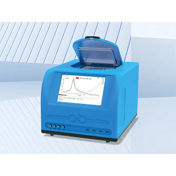
- Explore the DMS-2000 for precise material characterization.
Request High-Precision Testing Solutions
Get expert guidance and customized instruments for your functional materials project.