Why Measure the Bulk Density of Ceramic Substrates?
Technical News

Ceramic substrates, such as alumina (Al2O3) and aluminum nitride (AlN), are the backbone of high-power electronics and advanced packaging. While engineers often focus on their electrical and thermal specifications, the bulk density of the ceramic is a fundamental physical metric that underpins nearly all performance characteristics. Measuring bulk density is not merely a geometric check; it is a vital diagnostic tool for evaluating the quality of the ceramic sintering process.
The Impact of Density on Substrate Performance
Bulk density is the ratio of a material's mass to its total volume, including any internal pores. In ceramic manufacturing, the goal of sintering is to achieve maximum densification, approaching the material's theoretical density. A lower-than-expected bulk density indicates higher porosity—the presence of microscopic voids within the ceramic structure. This porosity degrades performance across three critical domains:
1. Thermal Conductivity
Pores act as thermal insulators. In power electronics, where ceramic substrates are relied upon to dissipate heat away from semiconductor junctions, even a small percentage of porosity can severely impede thermal conductivity, leading to localized hotspots and premature device failure.
2. Mechanical Strength
Ceramics are inherently brittle, and internal pores act as stress concentrators. A substrate with low bulk density is significantly more susceptible to cracking or catastrophic fracture under mechanical shock or the thermal cycling stresses typical in electronic packaging.
3. Electrical Reliability (Dielectric and Resistivity)
Porosity has a profound impact on a substrate's insulating properties. Voids can trap moisture and contaminants, creating pathways that drastically lower the material's volume resistivity and dielectric strength. This increases the risk of electrical breakdown under high voltage. Furthermore, porosity alters the material's dielectric constant, which can disrupt impedance matching in high-frequency RF circuits. Instruments like the DMS2000 and RMS-1000s are frequently used to trace these electrical degradation issues back to insufficient densification.
Testing Methods and Quality Assurance
Bulk density is typically measured using the Archimedes principle (water displacement method), which provides a highly accurate assessment of both apparent density and open porosity. For B2B manufacturers, integrating rigorous bulk density testing into the quality control pipeline ensures that only substrates meeting strict densification standards are passed on to the metallization and assembly stages. This proactive testing mitigates the risk of deploying structurally and electrically compromised components into mission-critical power systems.
Related Testing Solutions
Related Instruments & Equipment
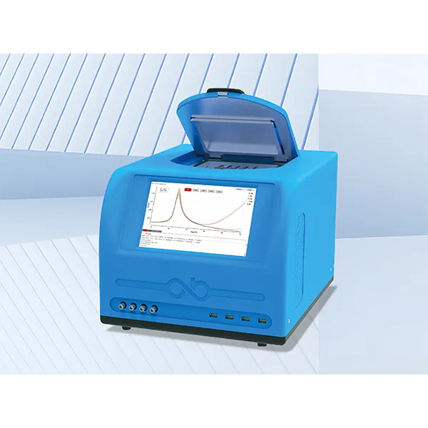
MatMeas DMS2000 High-Low Temperature Dielectric Spectrometer
The MatMeas DMS2000 is an advanced High and Low Temperature Dielectric Impedance Spectrometer engineered for evaluating the dielectric properties of materials under extreme thermal conditions. Compliant with the ASTM D150 standard, it integrates a proprietary LNP-95 liquid nitrogen injection system to achieve seamless continuous temperature variation from -160°C to 450°C. Uniquely featuring a vacuum-enabled sample chamber to completely prevent thermal frosting and eliminate false water peaks near 0°C, along with versatile options for single-sample or five-sample simultaneous testing, the DMS2000 ensures unparalleled data fidelity and high throughput for advanced scientific research.
View details →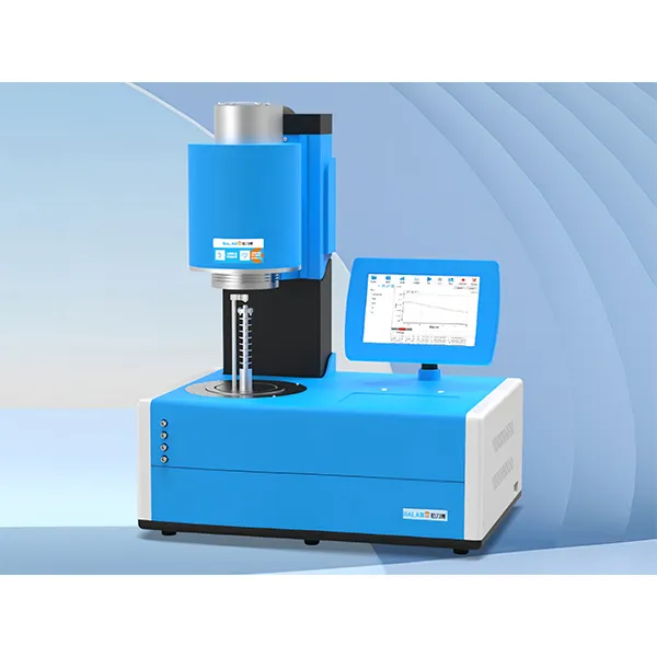
MatMeas RMS-1000S High-Temp Semiconductor Resistivity System
RMS-1000S is optimized for semiconductor bulk materials with four-wire method, offering 0.1mΩ~100MΩ measurement range, spring-loaded platinum electrodes, and multiple atmosphere environments for complex resistivity characterization.
View details →Request High-Precision Testing Solutions
Get expert guidance and customized instruments for your functional materials project.