High-Temperature Resistance and Resistivity Testing
Technical News
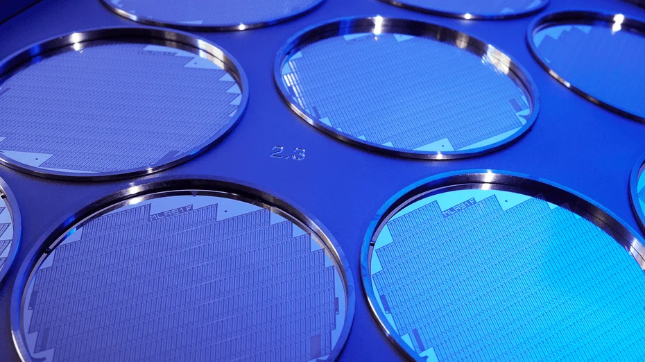
Accurate measurement of electrical resistance and volume resistivity at elevated temperatures is a foundational requirement across solid-state physics, high-temperature structural ceramics, wide-bandgap semiconductors (SiC, GaN), and solid oxide fuel cell (SOFC) electrolytes. As operating temperatures increase toward 1000°C and beyond, materials undergo profound changes in charge transport physics—transitioning from extrinsic band conduction to intrinsic thermal hopping, ionic vacancy migration, or grain boundary space-charge conduction.
However, executing high-temperature electrical metrology introduces severe experimental artifacts that routinely invalidate standard laboratory test setups. Thermally induced Seebeck electromotive forces (EMF) generate DC offset voltages, lead wire resistance dominates low-impedance measurements, electrode metallurgical reactions contaminate samples, and furnace atmospheric leakage current bypasses high-impedance specimens. Overcoming these barriers requires implementing rigorous four-wire Kelvin topologies, bipolar current commutation, and specialized high-temperature electrode metallization.
Fundamental Charge Transport Physics and Thermoelectric Error Decoupling
Electrical conduction in solid materials at elevated temperatures is broadly governed by electronic band transport or defect-mediated hopping. For semiconducting ceramics and ionic conductors, electrical conductivity σ(T) follows the Arrhenius thermal activation model:
σ(T) = (σ0 / T) · exp[−Ea / (kB · T)]
where σ0 represents the pre-exponential factor, Ea is the activation energy for electrical transport (in eV), kB is the Boltzmann constant (8.617 × 10⁻⁵ eV/K), and T is the absolute temperature in Kelvin. Taking the natural logarithm yields the classic Arrhenius relation:
ln(σ · T) = ln(σ0) − Ea / (kB · T)
Extracting the true specimen resistance RDUT is frequently corrupted by parasitic thermoelectric voltages. When dissimilar conductors (e.g., platinum probe wires contacting a conductive ceramic) operate across steep furnace temperature gradients (ΔT), the Seebeck effect generates a parasitic DC offset voltage VEMF:
Vmeasured = Isource · RDUT + VEMF = Isource · RDUT + SAB · ΔT
where SAB is the relative Seebeck coefficient between the lead wire and the test coupon. Under steady-state DC excitation, VEMF can easily exceed the actual resistive voltage drop by orders of magnitude, particularly when testing high-conductivity specimens at temperatures above 600°C.
To completely eliminate VEMF, modern metrology systems employ dynamic bipolar current commutation (current reversal). By applying alternating positive and negative current pulses (+Isource and −Isource), two sequential voltage readings are acquired:
Vforward = +Isource · RDUT + VEMF
Vreverse = −Isource · RDUT + VEMF
Subtracting the reverse measurement from the forward measurement algebraically cancels out the temperature-induced Seebeck offset voltage:
Vtrue = (Vforward − Vreverse) / 2 = Isource · RDUT
RDUT = Vtrue / Isource
Metrology Topology Selection: Two-Probe vs. Four-Probe vs. van der Pauw
The physical geometry of the test coupon and its anticipated resistance range determine the appropriate contact topology. Measuring low-resistance conductors or semiconductors with a conventional two-wire ohmmeter introduces catastrophic errors because the measured value includes probe contact resistance (Rc) and lead wire resistance (Rlead).
The comparative matrix below evaluates the three primary high-temperature electrical characterization methods:
| Metrology Topology | Electrode Configuration | Dominant Error Source | Typical Measurable Resistance Range | Specimen Geometry Constraints | Applicable International Standards |
|---|---|---|---|---|---|
| Two-Probe Configuration | 2 electrodes sharing current source and voltmeter | Lead wire resistance (Rlead) and contact barrier (Rc) | High to ultra-high (>100 kΩ up to 10¹⁴ Ω) | Planar discs, parallel plates with uniform cross-section | ASTM D257, IEC 60093 |
| Four-Wire Kelvin Method | 4 collinear or paired pins (outer force I, inner sense V) | Lead-wire Seebeck EMF; high contact impedance on sense pins | Ultra-low to moderate (10⁻⁶ Ω to 100 kΩ) | Rectangular bars, cylindrical rods with aspect ratio L/W > 5 | ASTM C611, SEMI MF84 |
| van der Pauw Technique | 4 point contacts placed on the perimeter of arbitrary shape | Non-uniform edge spacing, geometric boundary perturbation | Low to intermediate (10⁻³ Ω to 1 MΩ) | Uniform flat plates of arbitrary shape, continuous thickness t | ASTM F76, ISO 21712 |
For four-point collinear probe configurations on semi-infinite flat specimens, the volume resistivity ρ is derived using geometric correction factors F(w/s):
ρ = 2 · π · s · (V / I) · F(w/s)
where s represents probe pin spacing and w is specimen thickness. When specimen thickness w is significantly smaller than pin spacing s (w / s < 0.5), the relation converges to the thin-sheet limit:
ρ = (π / ln 2) · w · (V / I) ≈ 4.532 · w · (V / I)
High-Temperature Electrode Metallization and Paste Selection
The chemical and metallurgical stability of the electrical contact interface dictates measurement accuracy above 500°C. Incompatible electrode materials can oxidize, evaporate, diffuse into the bulk lattice, or form low-melting-point eutectic liquids that irreversibly destroy the specimen.
The electrode selection table below outlines performance boundaries for high-temperature conductive pastes:
| Metallization Paste Type | Max Continuous Temp in Air (°C) | Chemical Reactivity & Atmosphere Resistance | Sintering Temperature (°C) | Thermal Expansion Matching (CTE) | Preferred Substrate Applications |
|---|---|---|---|---|---|
| Colloidal Silver (Ag) | 600–650 | High risk of silver migration under DC field; volatilizes above 700°C | 450–550 | High (~19 × 10⁻⁶ /K); risk of thermal spalling | Low-temperature functional ceramics, ferrites |
| Organometallic Gold (Au) | 850–900 | Inert in air/O2; forms brittle eutectics with Si at 363°C; costly | 750–850 | Intermediate (~14 × 10⁻⁶ /K); good adhesion | High-frequency dielectrics, piezoceramics |
| Pure Platinum (Pt) | 1000–1600 | Completely non-oxidizing in air; inert with oxides; zero volatilization | 950–1100 | Moderate (~9 × 10⁻⁶ /K); excellent match to Al2O3 | Structural ceramics, solid electrolytes, SOFCs |
| Nickel / Nickel-Chrome | 800 (reducing only) | Rapidly oxidizes in ambient air; stable in Ar, N2, or vacuum | 800–900 | Moderate (~13 × 10⁻⁶ /K); economical | Non-oxide structural ceramics (SiC, Si3N4) |
International Standards Compliance & Experimental Best Practices
Executing verifiable high-temperature resistance testing requires adherence to standard operating procedures defined in ASTM C611 (Standard Test Method for Electrical Resistivity of Manufactured Carbon and Graphite Articles at Room and Elevated Temperatures) and ASTM D1829 (Standard Test Method for Electrical Resistance and Resistivity of Ceramic Materials at Elevated Temperatures).
Key experimental precautions include:
- Thermal Equilibrium Soak Time: High-temperature measurements must never be collected during rapid heating or cooling transients. A thermal stabilization dwell of at least 15 to 30 minutes at each temperature setpoint is mandatory to ensure the core of the ceramic reaches isothermal equilibrium with the furnace environment.
- Triaxial Shielding and Furnace Grounding: At temperatures exceeding 700°C, furnace heating elements emit thermionic electrons and electromagnetic hum that easily couple into high-impedance sense lines. Ceramic measurement fixtures must incorporate grounded refractory metal shields (Inconel or platinum) surrounding the specimen stage.
- Controlled Atmosphere Regulation: Oxide ceramics requiring specific defect stoichiometry (such as oxygen vacancy concentration in perovskites) must be tested under controlled oxygen partial pressure (pO2) environments using certified mass flow controllers.
Advanced Metrology Instrumentation: MatMeas RMS-1000S System
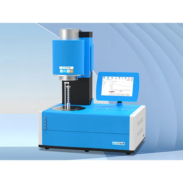
To address the demanding requirements of semiconductor materials, solid-state electrolytes, and thermoelectric alloys, the MatMeas RMS-1000S High Temperature Four-Probe Resistance Measuring System integrates closed-loop thermal regulation with high-precision electrical instrumentation.
Operating across a broad temperature span from ambient room temperature up to 1000°C (with ramps up to 10°C/min under ±0.5°C stability), the RMS-1000S utilizes spring-loaded platinum probe pins housed within a high-purity alumina tube fixture. This architecture prevents specimen warping while accommodating variable thermal expansion. The built-in commutation source unit switches current polarity at frequencies up to 10 Hz, suppressing Seebeck EMF and thermal drift across a measurement span from 10 μΩ to 100 MΩ. Automated software tracks resistance versus temperature, instantaneously generating Arrhenius plots and extracting electrical activation energies with zero manual calculation overhead.
Frequently Asked Questions
Why does a two-wire ohmmeter produce inaccurate measurements when testing conductive materials at high temperatures?
A two-wire ohmmeter passes test current through the same pair of leads used to sense voltage. The resulting measurement records the sum of lead resistance (Rlead), contact interface resistance (Rc), and the actual specimen resistance (RDUT). In high-temperature setups where long platinum or refractory leads operate inside a furnace, lead and contact resistances often reach several ohms, completely overwhelming the milliohm-range resistance of the test specimen. A four-wire Kelvin setup routes current through separate force leads while high-impedance sense leads measure voltage drop across the DUT without drawing current, eliminating lead and contact resistance artifacts.
How does Seebeck EMF corrupt high-temperature DC resistance data, and how is it corrected?
When probe leads contact a heated ceramic sample across an unavoidable thermal gradient inside the furnace tube, the thermocouple effect creates a DC voltage offset (Seebeck EMF). If an operator measures DC voltage under a single polarity, this thermal voltage adds algebraically to the true resistive drop (I · R), distorting resistance readings by up to 50% or more. High-precision systems eliminate this error by applying alternating bipolar current pulses (+I and −I) and calculating the difference (Vforward − Vreverse) / 2, which cancels out the Seebeck EMF component completely.
Which electrode metallization paste is recommended for oxide ceramics testing up to 1000°C in air?
Pure platinum (Pt) paste is the definitive choice for testing oxide ceramics up to 1000°C in air. Platinum exhibits zero oxidation across the entire temperature span, does not volatilize (unlike silver above 700°C), and matches the thermal expansion coefficient of alumina and perovskite ceramics closely. After screen printing or brush application, platinum paste must be sintered at 950°C–1050°C to burn off organic binders and form an electrically continuous, adherent porous network.
Request High-Precision Testing Solutions
Get expert guidance and customized instruments for your functional materials project.