Room-Temperature d33 Testing of Piezoelectric Films
Technical News
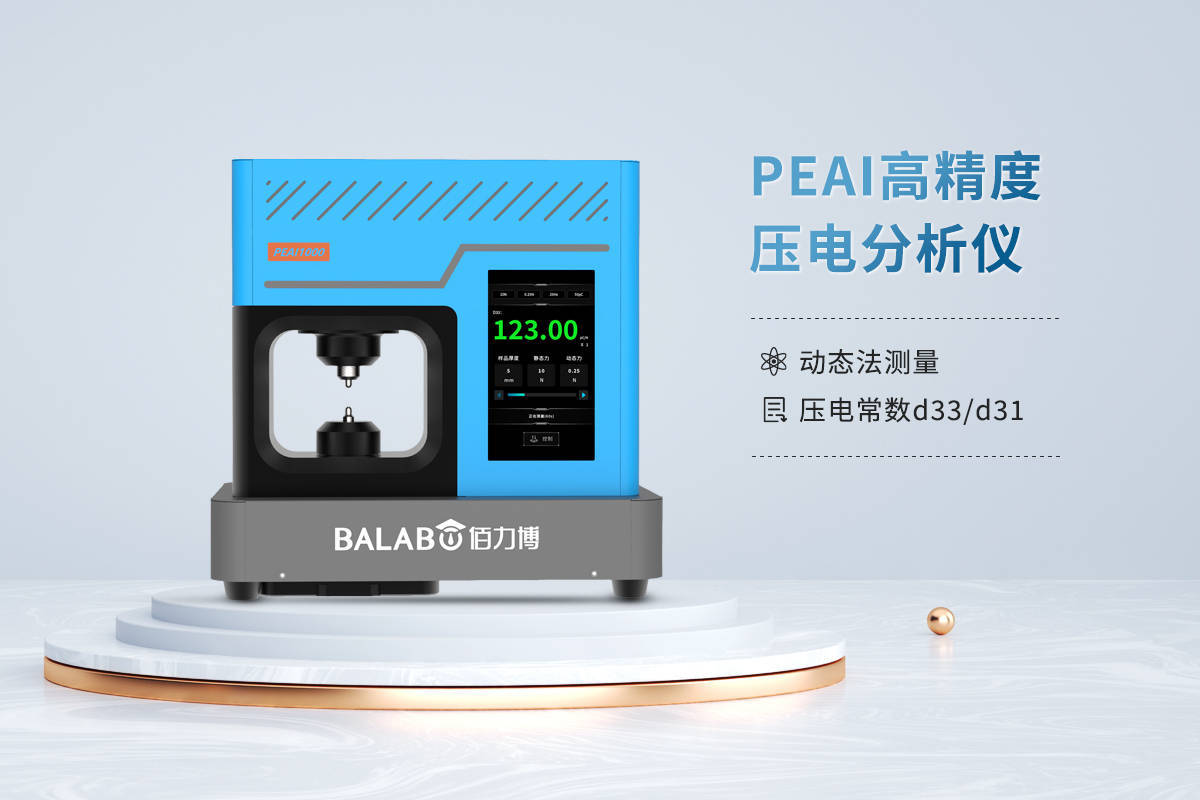
The longitudinal piezoelectric charge coefficient, d33, represents the primary figure of merit for functional electroceramic materials, quantifying the electrical charge generated per unit of applied mechanical force along the polarization axis (or reciprocally, the mechanical strain generated per unit of applied electric field). In contemporary microelectromechanical systems (MEMS), telecommunications radio-frequency (RF) filters, ultrasonic fingerprint sensors, and micro-actuators, piezoelectric thin films—typically ranging from 100 nanometers to several micrometers in thickness—have rapidly displaced bulky sintered ceramics.
Characterizing thin-film d33 at room temperature serves as the non-negotiable baseline for evaluating thin-film crystalline orientation, polarization efficiency, and mechanical integrity. However, transferring metrology from freestanding bulk ceramics to substrate-supported thin films introduces formidable physical complexities. A thin film deposited onto a silicon, sapphire, or glass substrate is mechanically clamped in the lateral plane, altering its constitutive electromechanical response. Accurately extracting the effective longitudinal piezoelectric coefficient (d33,f) and decoupling it from substrate bending, contact impedance, and mechanical compliance requires rigorous metrology grounded in IEEE and SEMI standards.
Mechanical Clamping and the Lefki-Dormans Constitutive Model
In bulk ceramic resonators, boundary conditions are typically unconstrained in all dimensions during low-frequency quasi-static characterization. In contrast, a thin film firmly adhered to a massive, passive substrate cannot deform freely in the lateral x-y directions. When an alternating electric field is applied along the out-of-plane z-axis (direction 3), the film attempts to expand laterally via its transverse piezoelectric coefficient d31. Because the substrate is orders of magnitude thicker (e.g., 500 micrometers of silicon versus 1 micrometer of piezoelectric film), the substrate enforces a zero-strain boundary condition in the film plane:
S_1 = S_2 = 0
This lateral constraint generates large in-plane mechanical stresses that couple back into the thickness strain through Poisson contraction, directly reducing the observed longitudinal displacement. To account for this mechanical clamping effect, Lefki and Dormans developed the classic constitutive model for thin-film longitudinal piezoelectricity:
d33,f = d33 - [ (2 * s13_E) / (s11_E + s12_E) ] * d31
where d33,f is the effective thin-film piezoelectric coefficient, d33 and d31 are the intrinsic, unconstrained piezoelectric charge coefficients, and s11_E, s12_E, and s13_E denote the elastic compliances of the piezoelectric film measured under constant electric field.
Because d31 typically exhibits the opposite algebraic sign to d33 in ferroelectric perovskites and wurtzite nitrides (and s13_E is negative), the clamping term consistently reduces the measurable displacement. For example, while bulk unconstrained lead zirconate titanate (PZT-5A) exhibits an intrinsic d33 exceeding 370 pC/N to 400 pC/N, its effective clamped thin-film counterpart d33,f typically caps at 60 pC/N to 120 pC/N. Understanding this constitutive disparity prevents researchers from misdiagnosing fundamental lattice clamping as film degradation or poor poling quality.
| Measurement Paradigm | Free Bulk Ceramic | Substrate-Clamped Thin Film |
|---|---|---|
| Mechanical Boundary Condition | Unconstrained stress-free boundary (T1 = T2 = T3 = 0) | Rigid planar strain clamping (S1 = S2 = 0, T3 != 0) |
| Longitudinal Coefficient | Intrinsic bulk d33 (pC/N or pm/V) | Effective clamped d33,f = d33 - [2*s13/(s11+s12)]*d31 |
| Poisson Contraction Feedback | Free lateral strain S1 = S2 = d31 * E3 | Constrained lateral strain; generates compressive/tensile stress |
| Typical Value Range | 150 pC/N to 600+ pC/N (PZT / relaxors) | 20 pC/N to 140 pC/N (PZT); 4 pC/N to 25 pC/N (AlN/ScAlN) |
| Substrate Flextensional Artifact | Negligible; homogeneous stress distribution | Severe; wafer bending creates parasitic bending charges |
| Governing Standard | IEEE Std 176, IEC 60483 | SEMI MS4-0307, IEEE Std 176 |
Benchmark Properties Across Key MEMS Piezoelectric Thin Films
Selecting thin-film materials for MEMS acoustic resonators, micropumps, and energy harvesters requires balancing effective piezoelectric response, dielectric permittivity, breakdown field, and mechanical quality factor.
| Thin-Film Material System | Crystal Symmetry / Deposition | Typical Film Thickness | Effective d33,f (pC/N) | Intrinsic Bulk d33 (pC/N) | Relative Permittivity (ε_r @ 1 kHz) | Electromechanical Coupling (kt^2, %) | Dielectric Loss (tanδ @ 1 kHz) | Primary MEMS Application Domain |
|---|---|---|---|---|---|---|---|---|
| Pure AlN (Aluminum Nitride) | Wurtzite (0002) / Reactive Sputtering | 0.5 - 2.0 µm | 4.5 - 5.5 | 5.5 | 9.0 - 10.5 | 6.0 - 7.0 | ≤ 0.003 | 5G Bulk Acoustic Wave (BAW/FBAR) filters |
| Sc0.2Al0.8N (Scandium Doped AlN) | Wurtzite (0002) / Co-sputtering | 0.5 - 1.5 µm | 12.0 - 16.0 | 18.0 - 24.0 | 13.0 - 16.0 | 12.0 - 15.0 | ≤ 0.006 | Wideband 5G/6G RF filters, PMUT arrays |
| Sc0.4Al0.6N (High-Sc AlN) | Highly strained wurtzite | 0.3 - 1.0 µm | 22.0 - 28.0 | 32.0 - 40.0 | 18.0 - 22.0 | 18.0 - 22.0 | ≤ 0.012 | Next-generation ultra-wideband acoustic resonators |
| Sol-Gel PZT (52/48 MPB) | Perovskite (100)/(111) / Sol-Gel | 1.0 - 3.0 µm | 70.0 - 110.0 | 300 - 450 | 800 - 1,400 | 10.0 - 14.0 | ≤ 0.030 | Micro-actuators, inkjet printheads, MEMS mirrors |
| Sputtered ZnO (Zinc Oxide) | Wurtzite (0002) / Magnetron Sputter | 1.0 - 4.0 µm | 8.0 - 10.5 | 12.4 | 8.5 - 11.0 | 7.0 - 8.5 | ≤ 0.010 | Surface acoustic wave (SAW) sensors, energy harvesters |
| P(VDF-TrFE) Copolymer | Ferroelectric Polymer / Spin Coating | 1.0 - 10.0 µm | -18.0 - -25.0 | -33.0 | 8.0 - 12.0 | 4.0 - 6.0 | ≤ 0.025 | Flexible tactile sensors, wearable biomedical patches |
The empirical benchmark illustrates the trade-offs across functional classes: while wurtzite aluminum nitride (AlN) exhibits lower absolute piezoelectric coefficients than ferroelectric PZT, its low dielectric constant (εr ≈ 10) and ultra-low dielectric loss (tanδ < 0.003) yield a superior acoustic figure of merit (kt^2 / tanδ), establishing it as the gold standard for high-frequency RF front-end filters.
Metrological Challenges: Substrate Bending and Static Force Drift
Accurate experimental extraction of thin-film d33,f is frequently corrupted by three major physical error sources:
- Substrate Flextensional Bending (Wafer Curvature Effect): When a normal point force is applied to a film-on-substrate specimen in a traditional Berlincourt clamp, the entire wafer flexes. Substrate bending introduces extensive lateral tensile strains in the film. Because the transverse coefficient
e31,f(e31,f = d31 / (s11_E + s12_E)) is large, the bending-induced charge overwhelms the pure longitudinal compressive charge, leading to measured d33 values that can be 200% to 500% higher than the true material property. - Contact Resistance and Puncturing: Applying uncalibrated mechanical preloads with sharp metallic probes easily punctures fragile thin-film top electrodes (typically 100 nm Au or Pt) or shatters brittle oxide films.
- Static Preload Drift and Charge Decay: Standard static force meters rely on steady-state charge integration. Dielectric leakage through micro-pinholes in the film bleeds off generated charges within milliseconds, causing apparent piezoelectric coefficients to decay toward zero.
Precision Dynamic Force Traceability via Lock-In Metrology
Eliminating substrate bending artifacts and leakage drift requires dynamic force direct traceability combined with phase-sensitive detection. High-precision characterization systems, such as the MatMeas PEMS-1000 thin-film piezoelectric analyzer, deploy a dynamic oscillatory mechanical excitation:
F(t) = F_static + F_dyn * sin(ω * t)
where F_static is a carefully regulated, non-destructive static bias force (typically 0.1 N to 0.5 N) to maintain continuous physical contact, F_dyn is a sinusoidal dynamic force (typically 0.05 N to 0.2 N), and ω is the excitation frequency swept between 30 Hz and 300 Hz.
The resulting piezoelectric charge generation follows:
Q(t) = Q_0 + d33,f * F_dyn * sin(ω * t + φ)
By routing this signal through a high-speed digital lock-in amplifier referenced to the mechanical drive frequency ω, static drift and low-frequency thermal fluctuations are rejected. Furthermore, by optimizing the mechanical tip radius and backing anvil geometry to ensure uniform, collinear force distribution across both faces of the substrate, local wafer bending modes are suppressed, isolating the genuine intrinsic longitudinal response.
Following baseline room-temperature validation, comprehensive reliability engineering requires tracking performance evolution across operating thermal envelopes. The MatMeas PMS-1000 piezoelectric temperature spectrum measurement system expands upon these room-temperature metrics by synchronizing dynamic mechanical loading with closed-loop PID thermal control. Incorporating an adaptive mechanical contact stage, the PMS-1000 accommodates thermal expansion mismatches between the substrate and ceramic film, preventing brittle delamination or cracking through phase transformations.
Standardized Specimen Preparation Guidelines
In accordance with SEMI MS4-0307 guidelines, rigorous sample preparation protocols must be maintained:
- Top Electrode Patterning: Top electrodes should be photolithographically patterned into discrete circular micro-pads (diameters between 200 µm and 1 mm). Measuring continuous unpatterned blanket films introduces severe lateral capacitive loading and lateral charge collection artifacts.
- Bottom Electrode Grounding: The bottom conducting electrode (e.g., Pt/Ti, TiN, or Mo) must possess a sheet resistance below 2 Ω/sq to prevent RC time constant attenuation during dynamic charge extraction.
- Substrate Backing Support: The specimen should be mounted on a polished, rigid tungsten carbide or hardened steel backing block to eliminate macroscopic wafer flexure during mechanical probe contact.
FAQ
Q: Why do traditional quasi-static Berlincourt d33 meters give wildly inaccurate readings on thin films?
A: Standard quasi-static meters apply heavy point clamping forces designed for bulk ceramics (several Newtons). On a thin film adhered to a silicon substrate, this point loading bends the substrate like a diaphragm. The resulting lateral bending strain activates the strong transverse piezoelectric coefficient (e31,f), generating parasitic charges that can be several times larger than the true longitudinal d33,f response. Specialized thin-film instruments like the MatMeas PEMS-1000 avoid this through dual-sided collinear micro-loading and phase-locked dynamic force modulation.
Q: What is the physical distinction between intrinsic d33 and effective d33,f?
A: Intrinsic d33 is the material property measured when the crystal lattice is completely unconstrained in all spatial directions (S1 = S2 = S3 != 0 under electric field). The effective coefficient d33,f describes the material clamped to a rigid substrate where in-plane strain is constrained to zero (S1 = S2 = 0). The substrate prevents lateral dimensional changes, inducing internal mechanical stresses that reduce the observable out-of-plane displacement via Poisson coupling, as modeled by the Lefki-Dormans equation.
Q: How does dynamic frequency selection (30 Hz to 300 Hz) improve measurement reliability?
A: Operating within a controlled 30 Hz to 300 Hz window avoids both low-frequency quasi-static DC charge leakage (which decays through finite film resistance) and higher-frequency acoustic resonances (which induce structural vibration modes). Phase-sensitive lock-in demodulation locks strictly onto the mechanical excitation frequency, rejecting ambient 50/60 Hz electrical noise and thermal drift to deliver clean, traceable pC/N data.
Related Instruments & Equipment
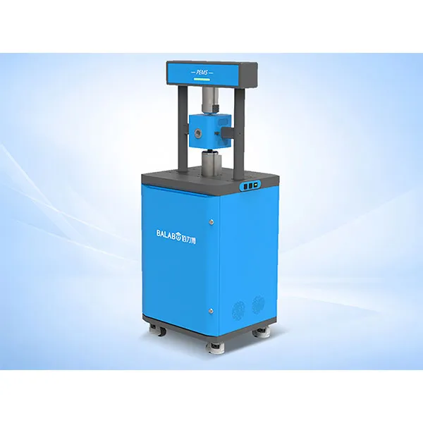
MatMeas High Precision In‑situ d33 Piezoelectric Measurement System – PEMS Analyzer
MatMeas PEMS is a high‑precision in‑situ d33 piezoelectric measurement system for advanced material characterization.
View details →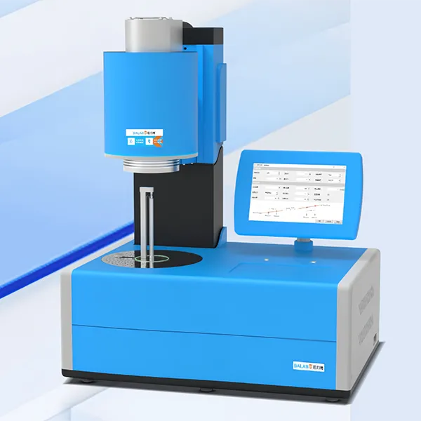
MatMeas PMS-1000 Piezoelectric Temperature Spectrum Measurement System
High-precision piezoelectric temperature spectrum measurement system for analyzing piezoelectric properties under varying temperatures.
View details →Request High-Precision Testing Solutions
Get expert guidance and customized instruments for your functional materials project.