TSDC Testing for In-Situ Polarization of Thin Films
Technical News
Thermally Stimulated Depolarization Current (TSDC) testing—historically also denoted in analytical literature as thermally stimulated discharge current or electret thermal analysis—is an advanced dielectric spectroscopy technique. It is engineered to probe localized defect states, defect-dipole reorientations, shallow and deep carrier trap distributions, and interfacial space charge dynamics in thin-film dielectrics.
As functional electronic devices scale down into the nanometer and micrometer regimes—exemplified by ferroelectric random-access memories (FeRAM), atomic-layer-deposited (ALD) high-k gate oxides (such as HfO2 and ZrO2), wide-bandgap passivating layers (Al2O3 and SiNx), and high-energy-density flexible polymer nanocomposites—microscopic charge trapping becomes the primary bottleneck governing device endurance. Trapped electrons, holes, and charged oxygen vacancies migrate under operating electric fields, accumulating at metal-dielectric interfaces or grain boundaries. This accumulation induces threshold voltage instability, dielectric fatigue, leakage current escalation, and premature breakdown.
While conventional AC broadband dielectric spectroscopy (BDS) provides valuable insight into high-frequency dipolar relaxations, its sensitivity decays drastically at ultra-low frequencies (< 10^-2 Hz), where slow defect relaxations and deep space-charge detrapping occur. TSDC effectively acts as an ultra-low equivalent frequency probe (resolving relaxation processes with equivalent frequencies down to 10^-5 Hz to 10^-6 Hz). By applying a four-stage thermodynamic protocol—polarization, cryogenic freezing, isothermal short-circuiting, and controlled linear thermal ramping—TSDC extracts ultra-weak picoampere and femtoampere discharge currents, providing an exquisitely sensitive fingerprint of electronic and ionic defect energetics.
The Four Thermodynamic Stages of Thin-Film TSDC Metrology
A rigorous TSDC measurement protocol is executed through four distinct, sequentially linked thermodynamic phases:
1. In-Situ High-Temperature Poling
The dielectric thin film is heated to an elevated poling temperature T_p (typically chosen below the irreversible decomposition or crystallization threshold, but sufficiently high to impart thermal mobility to defect dipoles and mobile charges). A calibrated DC poling field E_p (often 10 kV/mm to over 200 kV/mm for micro-scale films) is applied across the top and bottom micro-electrodes for a dwell time t_p (typically 10 to 30 minutes). Under this combined thermal and electrical excitation, three distinct polarization phenomena occur:
- Alignment of intrinsic and defect dipoles along the electric field vector.
- Drift and spatial separation of mobile charge carriers (ions, electrons, and vacancies) toward blocking electrode interfaces, forming localized space charge polarization.
- Direct charge injection from the metallic contact into near-surface dielectric traps via Fowler-Nordheim tunneling or Schottky emission.
2. Cryogenic Freezing Under Field
While maintaining the DC poling field E_p at full magnitude, the sample chamber is rapidly cooled at a rate of 10 C/min to 20 C/min down to a baseline cryogenic freezing temperature T_0 (typically -160 C via liquid nitrogen refrigeration). At this deeply depressed temperature, the thermal kinetic energy k_B * T drops far below the activation energy barrier E_a required for dipole rotation or charge detrapping. Consequently, the non-equilibrium polarization state is "frozen" into the dielectric lattice, where the relaxation time constant tau(T_0) extends to days or centuries.
3. Isothermal Short-Circuit Relaxation
Upon reaching T_0, the external DC voltage source is disconnected, and the thin-film electrodes are connected across a sensitive electrometer in a closed virtual-ground circuit for an isothermal relaxation period t_d (typically 5 to 15 minutes). This step allows fast geometric capacitive charges (Q = C * V) and very shallow surface charges to discharge completely, establishing a baseline current below 0.05 pA.
4. Controlled Linear Thermal Ramp and Current Detection
With the sample maintained in short-circuit configuration, the heating system executes a strictly linear temperature ramp at rate beta = dT/dt (typically 1 C/min to 5 C/min) up to the maximum test temperature. As thermal energy increases, frozen dipoles progressively regain rotational mobility, randomizing their orientations, while trapped carriers overcome their energy wells and recombine. The resulting movement of bound polarization charges induces a minute displacement and conduction current in the external circuit, generating a multi-peaked TSDC thermogram J(T).
Physical Constitutive Equations: The Bucci-Fieschi-Guidi (BFG) Model
The fundamental mathematical framework governing dipolar depolarization in solid dielectrics is formulated by the classic Bucci-Fieschi-Guidi (BFG) non-isothermal relaxation equation:
J(T) = (P_0 / tau(T)) * exp[ - (1 / beta) * integral_T0_T (1 / tau(T')) dT' ]
Assuming that the microscopic relaxation time tau(T) follows Arrhenius activation kinetics:
tau(T) = tau_0 * exp(E_a / (k_B * T))
Substituting the Arrhenius relation yields the full BFG depolarization current density equation:
J(T) = (P_0 / tau_0) * exp(-E_a / (k_B * T)) * exp[ - (1 / (beta * tau_0)) * integral_T0_T exp(-E_a / (k_B * T')) dT' ]
Where:
- J(T): The measured depolarization current density (A/m2).
- P_0: The initial equilibrium polarization frozen into the lattice at temperature T_p (C/m2).
- tau_0: The pre-exponential attempt-to-escape relaxation time factor (typically 10^-12 s to 10^-14 s for atomic dipoles).
- E_a: The activation energy or trap depth (eV).
- k_B: The Boltzmann constant (8.617 * 10^-5 eV/K).
- beta: The linear heating ramp rate (beta = dT/dt, in K/s or C/min).
- T_0: The initial cryogenic freezing temperature (K).
Differentiating the BFG equation with respect to temperature and setting dJ/dT = 0 yields the mathematical condition for the maximum current peak temperature T_m:
T_m^2 = (beta * E_a * tau_0 / k_B) * exp(E_a / (k_B * T_m))
This transcendental relation proves that the peak temperature T_m depends solely on the intrinsic trap energetics (E_a, tau_0) and the programmed heating rate beta, and is strictly independent of the poling field E_p for linear dipolar relaxations.
Analytical Extraction of Trap Depth: The Garlick-Gibson Method
To extract the trap activation energy E_a from experimental TSDC data without solving the complex integral over the entire peak profile, researchers employ the Garlick-Gibson initial rise method. In the initial low-temperature ascent of the TSDC peak (where T << T_m and the accumulated current is less than 10% of the peak maximum J_max), the integral term in the BFG equation remains approximately equal to zero:
exp[ - (1 / (beta * tau_0)) * integral_T0_T exp(-E_a / (k_B * T')) dT' ] roughly equals 1
Under this low-temperature boundary condition, the current density simplifies to:
J(T) roughly equals (P_0 / tau_0) * exp(-E_a / (k_B * T))
Taking the natural logarithm of both sides:
ln[J(T)] = C - (E_a / k_B) * (1 / T)
Where C = ln(P_0 / tau_0) is a constant. Plotting ln[J(T)] versus the inverse absolute temperature (1/T) yields a straight line whose slope m is directly proportional to the trap activation energy:
E_a = -k_B * m = -k_B * (d(ln J) / d(1/T))
Furthermore, the total trapped charge density Q_trap and the volumetric defect trap state density N_t within a film of thickness d_film are extracted by integrating the area under the entire TSDC peak:
Q_trap = (1 / beta) * integral_T_initial^T_final J(T) dT
N_t = Q_trap / (q * d_film)
Where q is the elementary electron charge (1.602 * 10^-19 C).
Deconvolution of Complex TSDC Spectra: Peak Assignment Matrix
In polycrystalline thin films and multi-component nanocomposites, a raw TSDC thermogram rarely consists of a single isolated peak. Instead, multiple overlapping peaks emerge across the cryogenic-to-high-temperature sweep. The following diagnostic matrix details how to distinguish between dipolar, space-charge, and interfacial Maxwell-Wagner-Sillars (MWS) relaxations.
| Peak Nomenclature | Physical Origin | Typical Temperature Window | Peak Shift vs. Heating Rate beta | Peak Height vs. Poling Field E_p | Decoupling & Diagnostic Criteria |
|---|---|---|---|---|---|
| gamma-Peak (Cryogenic) | Localized sub-group or side-chain dipole oscillations | -160 C to -80 C | Shifts upward by 5 C to 10 C as beta increases | Linear with E_p (P_0 proportional to E_p) | Reversible; identical on repeated runs; low activation energy (0.15 eV to 0.35 eV) |
| beta-Peak (Sub-Ambient) | Shallow electron/hole trapping at grain boundaries | -80 C to +20 C | Shifts upward moderately with increasing beta | Linear or weak power law (E_p^1.2) | Quenched by illumination with bandgap light; activation energy ~0.4 eV to 0.7 eV |
| alpha-Peak (Glass / Curie) | Main-chain dipolar relaxation or ferroelectric domain depoling | +50 C to +150 C | Strongly shifts upward with increasing heating rate | Strictly linear with E_p up to ferroelectric saturation | Corresponds precisely to dielectric loss tan delta peak in AC impedance spectroscopy |
| rho / Space Charge Peak | Deep bulk trapping (e.g., oxygen vacancy migration) | +150 C to +300 C | Shifts upward; peak shape broadens significantly | Non-linear with E_p (E_p^1.5 to E_p^2.0) | Shifts to lower T with increasing poling time t_p; activation energy 0.9 eV to 1.4 eV |
| Maxwell-Wagner-Sillars (MWS) | Interfacial carrier accumulation at dielectric-metal contact | +250 C to +450 C | Complex shift; often obscured by high-temp leakage | Highly non-linear; depends strongly on electrode work function | Inverted polarity observed if blocking electrode boundary conditions are altered |
Benchmark Comparison: Thin-Film Dielectric Trap Parameters
The following table summarizes experimentally verified trap depths, relaxation time factors, and characteristic TSDC peak regimes across key thin-film technological systems.
| Material System | Film Architecture & Thickness | Primary Defect / Trapping Mechanism | Dominant Peak Temp T_m (at 3 C/min) | Extracted Trap Depth E_a (eV) | Pre-Exponential Factor tau_0 (s) | Volumetric Trap Density N_t (cm^-3) | Impact on End-Device Reliability |
|---|---|---|---|---|---|---|---|
| ALD Hafnia (HfO2) | 10 nm Si-doped MIM capacitor | Doubly ionized oxygen vacancies (V_O_ddot) | +185 C | 1.15 to 1.28 | 2.5 * 10^-13 | 4.0 * 10^18 | Governs threshold voltage drift and TDDB lifetime in FeRAM and logic gates |
| ALD Alumina (Al2O3) | 25 nm passivation film on Si | Interfacial dangling bonds and Al interstitials | +95 C | 0.82 to 0.94 | 8.0 * 10^-12 | 1.2 * 10^17 | Dictates surface recombination velocity in PERC solar cells and GaN HEMTs |
| P(VDF-TrFE) 70/30 | 1.2 um spin-coated polymer film | Dipolar crystalline-amorphous boundary traps | +65 C (alpha), +115 C (Curie) | 0.65 (alpha), 1.45 (Curie) | 5.0 * 10^-11 | 8.5 * 10^16 | Determines remanent polarization retention in flexible organic ferroelectrics |
| Sputtered BST Thin Film | 200 nm (Ba_0.7 Sr_0.3)TiO3 | Point defect complexes and grain boundary barriers | +220 C | 1.35 to 1.50 | 1.2 * 10^-14 | 6.0 * 10^18 | Limits high-temperature leakage in dynamic random-access memory (DRAM) cells |
| High-Temp Polyimide (PI) | 15 um spin-coated aerospace film | Imide ring defect dipoles and absorbed moisture | -50 C (moisture), +210 C (bulk) | 0.38 (dipole), 1.22 (space) | 3.0 * 10^-12 | 3.5 * 10^15 | Determines high-voltage partial discharge endurance in traction motor windings |
Hardware Architecture: Solving Probe Station Metrological Bottlenecks
Thin-film TSDC measurements present severe instrumentation challenges. Depolarization currents in sub-micron films typically range from 10^-14 A (10 fA) to 10^-11 A (10 pA). Because the measurement must be conducted over a wide temperature ramp (from -160 C to +450 C), physical thermal expansion and laboratory vibrations can easily displace micro-manipulated probe tips, causing intermittent contact or massive microphonic current spikes.
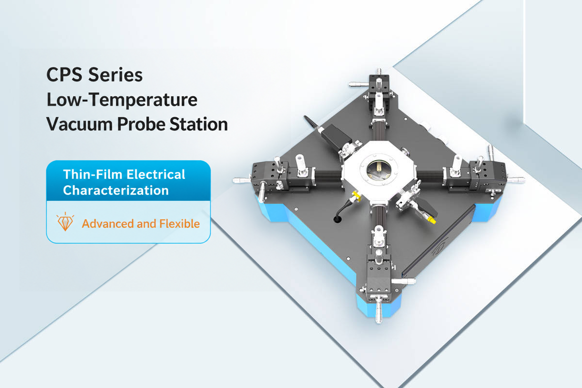
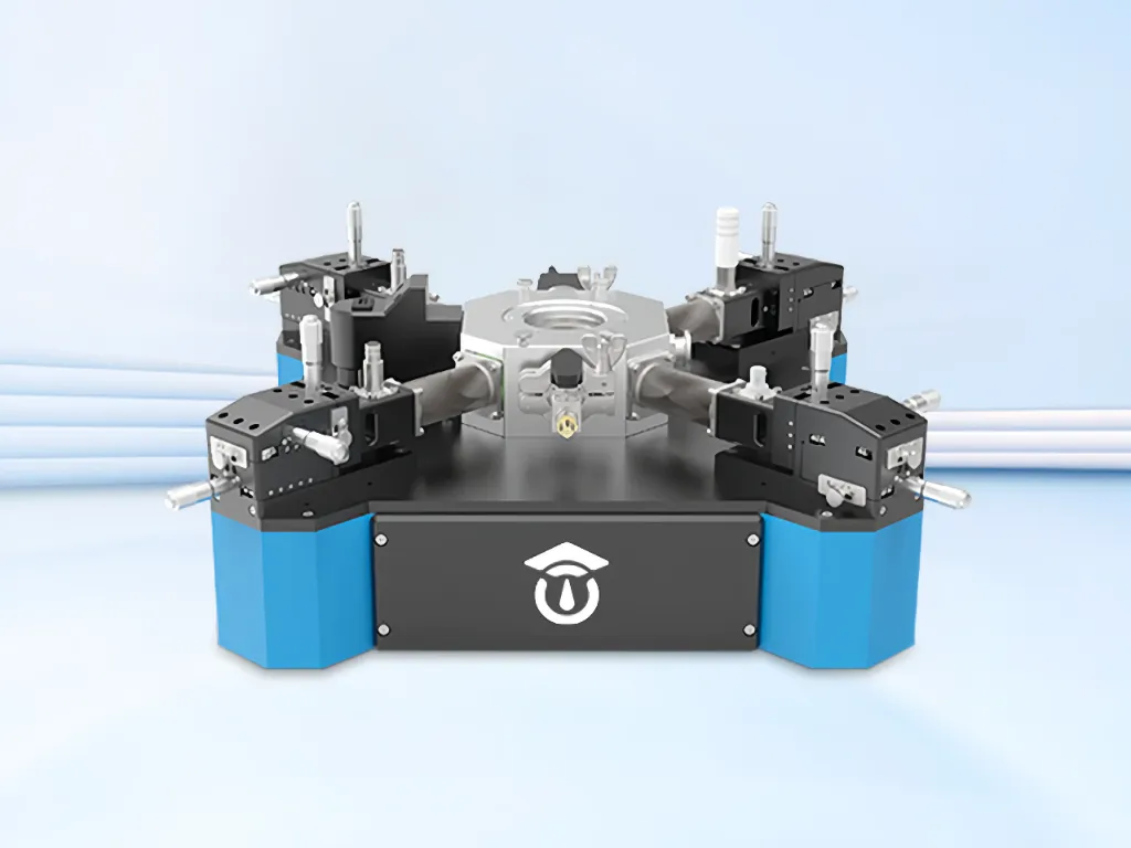
The MatMeas CPS-7000 High-Low Temperature Dielectric Vacuum Probe Station provides an integrated metrology environment engineered to overcome these challenges. The CPS-7000 incorporates an internal pneumatic air-shock vibration isolation suspension, eliminating external table rumble and floor harmonics down to 1.5 Hz. This allows tungsten or beryllium-copper micro-probes to maintain constant contact with micro-scale electrode pads (down to 20 um x 20 um) without scratching thin film layers during severe thermal expansion sweeps.
Operating under a clean high-vacuum environment (< 10^-3 Pa), the CPS-7000 eliminates atmospheric moisture condensation during cryogenic cooling to -160 C and prevents electrode oxidation during ramping up to +450 C. Its liquid nitrogen cryogenic cold-finger coupled with a low-noise non-inductive cartridge heater delivers linear heating ramp rates precisely programmable from 0.5 C/min to 10.0 C/min, with temperature uniformity across the 4-inch sample chuck held within +/-0.1 C. An integrated triaxial guard routing architecture isolates the electrometer signal path from furnace heater electromagnetic interference, lowering system baseline noise floor below 10 fA RMS.
Standardized Step-by-Step SOP for Thin-Film TSDC Characterization
To obtain publication-grade, mathematically deconvolutable TSDC thermograms, researchers must adhere to this standardized experimental procedure:
Step 1: Device Micro-Fabrication and Electrode Inspection
- Fabricate thin-film metal-insulator-metal (MIM) test structures on polished silicon or sapphire substrates. Recommended top electrode diameter is 100 um to 500 um to keep total capacitance manageable while generating measurable TSDC current.
- Verify electrode edges under optical microscopy to ensure no burrs, pinholes, or edge overhangs that might cause premature electrical breakdown under the poling field E_p.
- Clean the specimen with electronic-grade solvents, bake at 120 C for 30 minutes, and mount onto the vacuum chuck of the probe station.
Step 2: Vacuum Chamber Evacuation and Micro-Probing
- Close the probe station chamber and evacuate using a turbomolecular pumping station to a base pressure below 1.0 * 10^-3 Pa.
- Through the top quartz observation window, manipulate the triaxially shielded probe arms to land probe tips gently onto the top and bottom electrode pads, applying minimal mechanical contact force (< 0.05 N).
- Connect a precision electrometer and verify that the ambient noise floor is below 20 fA under zero applied bias.
Step 3: High-Temperature Poling and Cryogenic Freezing
- Heat the sample chuck to the target poling temperature T_p (e.g., 100 C) at a ramp rate of 5 C/min.
- Apply the DC poling electric field E_p (e.g., 50 kV/mm) for a duration of t_p = 15 minutes.
- While maintaining E_p continuously, open the liquid nitrogen cryo-valve to rapidly freeze the sample down to T_0 = -160 C at a rate of 15 C/min.
Step 4: Short-Circuiting and Linear Ramp Data Acquisition
- Switch the electrometer circuit to short-circuit mode (V = 0) and allow an isothermal dwell period of t_d = 10 minutes at -160 C to discharge transient capacitive currents.
- Initiate the linear thermal ramp at a constant, highly regulated rate (e.g., beta = 3.0 C/min) from -160 C to +350 C.
- Continuously log the depolarization current I_TSDC, current density J = I / A_electrode, absolute temperature T, and heating rate beta at a sampling frequency of at least 2 Hz.
- Apply the Garlick-Gibson slope analysis on the rising edge of each resolved peak to calculate the individual activation energy E_a and total trapped charge density Q_trap.
Frequently Asked Questions (FAQ)
Why is TSDC superior to standard AC dielectric spectroscopy for characterizing deep traps?
Standard AC broadband dielectric spectroscopy is constrained by measurement frequency. Detecting slow defect relaxations with time constants of minutes or hours requires probing at frequencies below 10^-3 Hz, where instrumental drift and conductive loss overwhelm the response. TSDC converts time-dependent relaxation into a temperature-dependent spectrum, resolving equivalent frequencies down to 10^-6 Hz and isolating deep trap states that cannot be separated by AC methods.
How do researchers confirm that a TSDC peak originates from dipoles rather than injected space charges?
Dipolar relaxation peaks exhibit two defining experimental characteristics: first, the peak current height J_max scales strictly linearly with the poling electric field E_p (because dipole alignment follows the Langevin function P_0 proportional to E_p in the weak-field limit). Second, the peak temperature T_m remains constant regardless of poling field magnitude or poling time t_p. In contrast, space-charge detrapping peaks exhibit non-linear field dependence and shift to different temperatures as poling conditions vary.
Why is an anti-vibration probe station design mandatory for thin-film TSDC?
Depolarization currents generated by micro-scale thin-film electrodes are exceptionally small (often between 10 fA and 1 pA). As the sample stage undergoes extreme temperature excursions from -160 C to +450 C, thermal expansion induces mechanical stress at the probe-substrate interface. Any external building vibrations or table movement will cause micro-probe slipping, creating triboelectric and microphonic noise spikes that completely destroy the delicate TSDC curve.
Can TSDC distinguish between bulk dielectric traps and electrode interfacial effects?
Yes, by systematically altering the measurement boundary conditions. By testing specimens with different film thicknesses under the same poling field, bulk dipolar and trap phenomena scale proportionally with film volume, whereas interfacial charge phenomena remain thickness-invariant. Furthermore, swapping top electrode metallizations (e.g., comparing high-work-function platinum against lower-work-function aluminum) shifts interfacial injection peaks while leaving bulk dipolar alpha-peaks unaffected.
Request High-Precision Testing Solutions
Get expert guidance and customized instruments for your functional materials project.