Volume Resistivity Testing of Solid Insulating Materials: Guarded Three-Electrode Method
Technical News

Volume resistivity testing of solid electrical insulating materials represents one of the most vital quality assurance and material qualification procedures in modern electrical engineering. Solid dielectrics—ranging from technical ceramics and mica laminates to cross-linked polyethylene (XLPE) cable jackets, fluoropolymers (PTFE), polyimide aerospace films, and epoxy encapsulation resins—must reliably isolate high voltages under harsh operational conditions.
The fundamental physical metric defining this capability is volume resistivity (rho_v, expressed in ohmcm or ohmm). It quantifies a dielectric's intrinsic bulk resistance to the passage of direct electric current per unit cross-sectional area and unit thickness.
However, accurately measuring true volume resistivity in high-performance insulating solids (where bulk resistance routinely spans 10^12 ohm to 10^16 ohm) is notoriously challenging. In an open laboratory environment, relative humidity deposits an invisible, nanometer-thick water film across the specimen surface. Because surface resistivity (rho_s) is frequently four to six orders of magnitude lower than bulk volume resistivity, electrical current preferentially flows across the exterior edges of the sample. In a basic two-electrode test, this superficial leakage shunts the bulk current, causing generic electrometers to register falsely depressed resistance readings with errors exceeding 1000%.
To eliminate surface leakage currents and isolate true volumetric conduction, international metrology bodies have standardized the guarded three-electrode test configuration under ASTM D257, IEC 62631-3-1, and ISO 2951.
Operating Principle of the Guarded Three-Electrode System
The guarded three-electrode architecture physically and electrically decouples surface leakage currents from internal volumetric currents by creating an active, equipotential boundary on the specimen surface:
- Electrode 1 (Guarded Measuring Electrode): Positioned coaxially on the top surface of the solid dielectric disc, having outer diameter d1. This electrode collects the pure volumetric current I_v flowing perpendicularly through the thickness h and routes it into the high-gain electrometer/picoammeter.
- Electrode 2 (Guard Ring Electrode): An annular ring encircling the center measuring electrode on the same top face. It is separated from Electrode 1 by a narrow annular guard gap of uniform width g. The guard ring is tied directly to the virtual-ground guard terminal of the electrometer system.
- Electrode 3 (Unguarded High-Voltage Counter Electrode): Covers the opposing bottom face of the specimen, having an outer diameter d3 greater than or equal to the outer perimeter of the guard ring. It connects directly to the programmable DC excitation power supply (typically sourcing 100 V to 1000 V DC).
When high voltage V is applied to Electrode 3, two distinct current circuits are established:
- Bulk Conduction Path: Current traverses vertically through the ceramic or polymer volume into Electrode 1, where the sensitive measuring circuit records the true bulk volume current I_v.
- Surface Leakage Path: Current emerging from the bottom face or creeping across the perimeter edges traverses the annular gap toward Electrode 2. Because Electrode 2 is tied to the low-impedance guard potential, all surface leakage current I_s is shunted harmlessly to ground without passing through the electrometer's measurement shunt resistor.
Furthermore, because Electrode 1 and Electrode 2 are maintained at virtually the exact same electrical potential (differing by less than 10 microvolts at the virtual-ground electrometer input), the lateral potential gradient across the annular gap g is virtually zero. Consequently, zero lateral surface current flows between the guard ring and the center electrode, ensuring 100% pure volume isolation.
ASTM D257 Mathematical Equations and Fringing Field Corrections
To calculate volume resistivity rho_v from the measured volume resistance R_v (R_v = V / I_v), the physical geometry of the electrode cell must be converted into an effective cross-sectional area A_eff.
Under ASTM D257 and IEC 62631-3-1, the volume resistivity is formulated as:
rho_v = R_v * (A_eff / h) = (V / I_v) * (A_eff / h)
Where:
- V: The applied steady-state DC test voltage (volts).
- I_v: The steady-state volume conduction current (amperes).
- h: The average thickness of the solid dielectric specimen (centimeters or meters).
- A_eff: The effective area of the guarded center measuring electrode.
Effective Electrode Area and Annular Gap Splitting
Because the electric field lines traversing the dielectric specimen do not truncate abruptly at the perimeter edge of Electrode 1, the electric field fringes across the annular gap g. ASTM D257 establishes that the effective diameter d_eff splits the annular gap symmetrically along its centerline:
d_eff = d1 + g - 2 * delta
Where d1 is the diameter of Electrode 1, g is the annular gap width (g = (d2 - d1) / 2), and delta is a fringing field correction term. For the vast majority of practical measurements where the annular gap width g is substantially smaller than the sample thickness h (g < 0.2 * h), delta is practically zero, and the effective diameter simplifies to:
d_eff approx d1 + g
The effective area A_eff is consequently calculated as:
A_eff = (pi / 4) * (d_eff)^2 = (pi / 4) * (d1 + g)^2
When high precision is demanded on thicker samples where the gap width g is comparable to or larger than thickness h, the exact fringing correction delta derived from conformal mapping is applied:
delta = (2 * h / pi) * ln[cosh(pi * g / (4 * h))]
Surface Resistivity Equation
When the instrument switches configurations to evaluate surface resistivity rho_s, the DC voltage is applied between the center measuring electrode (Electrode 1) and the guard ring (Electrode 2), while the bottom counter electrode (Electrode 3) serves as the guard shield. The surface resistivity (expressed in ohms per square, ohm/sq) is calculated as:
rho_s = R_s * (P_eff / g) = (V / I_s) * [pi * (d1 + g) / g]
Where P_eff = pi * (d1 + g) represents the effective perimeter along the centerline of the annular gap.
Standardized Geometry Specifications: ASTM D257 and IEC 62631-3-1
To ensure reproducibility across commercial laboratories, standard dimensions for electrode cells are strictly codified. The table below outlines standard electrode cell configurations.
| Standard Specification Cell Size | Center Electrode Diameter d1 (mm) | Guard Ring Inner Diameter d2 (mm) | Annular Gap Width g (mm) | Counter Electrode Diameter d3 (mm) | Maximum Specimen Thickness h (mm) | Recommended Test Voltage Span | Primary Material Category |
|---|---|---|---|---|---|---|---|
| Small Cell (Type A - Thin Films) | 25.0 +/- 0.1 | 27.0 +/- 0.1 | 1.0 +/- 0.05 | >= 35.0 | 0.05 to 1.5 mm | 10 V to 250 V DC | Polyimide, PET, fluoropolymer capacitor films, thin ceramic membranes |
| Medium Cell (Type B - Substrates) | 50.0 +/- 0.2 | 54.0 +/- 0.2 | 2.0 +/- 0.10 | >= 70.0 | 0.5 to 3.0 mm | 100 V to 500 V DC | Alumina (Al2O3), AlN, Si3N4 power substrates, rigid PCB laminates |
| Large Cell (Type C - Bulk Solids) | 100.0 +/- 0.5 | 110.0 +/- 0.5 | 5.0 +/- 0.20 | >= 120.0 | 2.0 to 10.0 mm | 500 V to 1000 V DC | High-voltage porcelain, epoxy castings, silicone rubber insulators |
Time-Dependent Dielectric Absorption and the 60-Second Rule
A fundamental source of operator error in volume resistivity metrology is recording current immediately upon voltage application. Solid dielectrics are not simple ohmic resistors; they are complex dielectric media exhibiting time-dependent polarization currents.
Upon applying a DC step voltage V, the total instantaneous current I_total(t) entering the material consists of three distinct physical components:
I_total(t) = I_geom(t) + I_absorp(t) + I_cond
- Geometric Capacitive Current (I_geom): The instantaneous charging current required to establish the electrostatic field across the vacuum capacitance C_0 of the cell (I_geom = C_0 * (dV/dt)). This current decays exponentially within milliseconds according to the circuit time constant tau_c = R_source * C_0.
- Dielectric Absorption Current (I_absorp): Arising from reversible dipole orientation, molecular segment relaxation, and interfacial Maxwell-Wagner-Sillars (MWS) polarization. Governed by the empirical Curie-von Schweidler law:
I_absorp(t) = A_0 * t^(-n)
Where A_0 is a polarization constant and the decay exponent n typically ranges between 0.7 and 1.0. This absorption current decays gradually over seconds, minutes, or even hours. 3. True Steady-State Conduction Current (I_cond): The non-decaying current resulting from intrinsic and extrinsic mobile ions, electrons, and defect vacancy hopping through the bulk volume (I_cond = V / R_v).
If an operator logs the current after only 5 seconds of electrification, the measured current is dominated by transient absorption current I_absorp(t), resulting in an apparent volume resistivity that is one to three orders of magnitude lower than the true material property. To establish a universal benchmark, ASTM D257 and IEC 62631-3-1 mandate a standard electrification time of exactly 60 seconds (1 minute +/- 1 second) before reading the final volume current I_v.
Benchmark Comparison: Solid Insulating Materials Across Temperature
The following table provides verified volume resistivity, dielectric properties, and high-temperature insulation degradation benchmarks across standard engineering dielectrics.
| Solid Insulating Material | Chemical / Structural Family | Volume Resistivity at 25 C (ohm*cm) | Volume Resistivity at 300 C (ohm*cm) | Relative Permittivity (1 kHz, 25 C) | Dielectric Loss (tan delta at 1 kHz) | Maximum Continuous Service Temp | Typical High-Voltage Insulation Application |
|---|---|---|---|---|---|---|---|
| Fused Quartz / Silica | High-purity amorphous SiO2 | > 1.0 * 10^17 | 5.0 * 10^11 | 3.8 | 0.0001 | 1100 C | Optical sensor windows, vacuum feedthroughs, semiconductor furnace tubes |
| High-Purity Alumina 99.8% | Polycrystalline alpha-Al2O3 | 5.0 * 10^15 | 2.0 * 10^11 | 9.9 | 0.0002 | 1600 C | High-voltage spark plugs, power semiconductor packages, laser submounts |
| Polytetrafluoroethylene (PTFE) | Fluoropolymer (Teflon) | > 1.0 * 10^18 | 1.0 * 10^13 (at 250 C) | 2.1 | < 0.0002 | 260 C | High-frequency RF coaxial cables, aerospace wiring insulation, chemical seals |
| Polyimide (Kapton HN) | Aromatic polyimide film | 1.5 * 10^16 | 2.0 * 10^10 | 3.4 | 0.0018 | 400 C | Traction motor slot liners, flexible printed circuits (FPC), satellite blankets |
| Electrical Grade Muscovite Mica | Hydrated aluminum potassium silicate | 1.0 * 10^15 | 8.0 * 10^9 | 6.5 to 7.5 | 0.0015 | 600 C | Generator coil wrap, high-temperature heating element supports, fire-resistant cables |
| Bisphenol-A Epoxy Resin | Cross-linked cycloaliphatic epoxy | 1.0 * 10^15 | 1.0 * 10^7 (degrades) | 3.6 to 4.2 | 0.0080 | 180 C | Switchgear bushings, dry-type transformer potting, composite insulators |
High-Temperature In-Situ Testing Platform: MatMeas HTS-1000HR
While ambient room-temperature measurements are sufficient for incoming material inspection, evaluating solid dielectrics for aerospace, defense, and electric vehicle traction drives demands variable-temperature testing up to +800 C. Above 300 C, generic laboratory test cells fail completely: their stainless steel electrodes oxidize, causing erratic contact resistance, while the ceramic insulators used to mount the cell degrade and become conductive, creating massive parallel leakage shunts that mask the specimen's actual volume resistance.
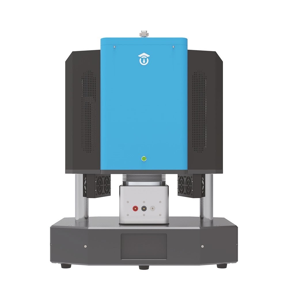
The MatMeas HTS-1000HR High Temperature Resistivity Measurement System is purpose-built to eliminate these high-temperature limitations. The HTS-1000HR integrates an active three-ring platinum electrode fixture constructed from ultra-high-purity (99.8%) recrystallized corundum and single-crystal sapphire isolators, maintaining complete dielectric isolation at temperatures up to +800 C.
The system features an automated motorized sample-loading stage with real-time feedback, applying a calibrated micro-clamping force of just 0.25 N. This ensures intimate electrical contact between the platinum electrodes and the sample face without cracking fragile, brittle technical ceramics or thin single crystals. To prevent electrode degradation and eliminate air ionization currents, the HTS-1000HR incorporates a vacuum-sealed environmental chamber capable of operating down to 10^-3 Pa, as well as under flowing dry nitrogen or argon. Its low-noise triaxial electrometer resolves ultra-weak currents down to 10 fA, providing high accuracy across the entire 10^3 ohm to 10^15 ohm resistance envelope.
Standardized Step-by-Step SOP for Three-Electrode Testing
To ensure full compliance with ASTM D257 and IEC 62631-3-1, testing technicians should adhere strictly to this experimental SOP:
Step 1: Specimen Slicing and Surface Preparation
- Fabricate specimens as circular discs (recommended diameter 50.0 mm to 60.0 mm) or square plates. Ensure opposing faces are ground flat and parallel to within +/-0.005 mm.
- Measure specimen thickness h at five distributed locations (center and four quadrants) using a calibrated digital micrometer; calculate and record the arithmetic mean thickness h.
- Clean the specimen ultrasonically in electronic-grade acetone for 10 minutes, followed by 10 minutes in isopropanol. Bake at 110 C for 1 hour to drive off moisture, then cool inside a desiccator.
Step 2: Electrode Application
- Option A (Fired-On Silver / Sputtered Metal): Use a precision shadow mask to apply the center electrode (d1 = 25.0 mm or 50.0 mm), guard ring (gap g = 1.0 mm or 2.0 mm), and bottom counter electrode. Sputter 100 nm of gold/platinum or fire silver paste according to standard thermal profiles.
- Option B (Conductive Silicone Rubber Contacts): For non-destructive testing of raw sheets, place precision die-cut conductive silicone rubber discs backed by polished metal plates against the sample faces.
Step 3: Fixture Assembly and Guard Connection
- Place the specimen centrally onto the bottom high-voltage electrode (Electrode 3).
- Lower the guarded measuring head, aligning Electrode 1 and the guard ring Electrode 2 coaxially over the metallized patterns. Apply a uniform mechanical contact force (0.25 N to 0.50 N).
- Connect low-noise triaxial cables: core to measuring electrode, inner shield to guard ring, and outer shield to instrument chassis earth. Close the Faraday shielding cage.
Step 4: Voltage Application and Electrification Timing
- Program the DC voltage source to 100 V DC (or 500 V DC).
- Apply voltage and immediately start an automated digital timer.
- Monitor the current decay curve. Log the final volume current I_v at exactly t = 60 seconds.
- Calculate volume resistivity rho_v using the effective area formula: rho_v = (V / I_v) * [(pi / 4) * (d1 + g)^2 / h].
- Discharge the sample through a 100 kOhm grounding resistor for at least 120 seconds before opening the chamber to guarantee operator safety.
Frequently Asked Questions (FAQ)
What is the exact physical function of the guard ring electrode in ASTM D257?
The guard ring electrode encircles the center measuring electrode on the same face of the specimen and is held at the same potential (virtual ground). Because there is virtually zero voltage drop across the narrow gap between the measuring electrode and guard ring, surface currents cannot flow into the ammeter. Instead, surface currents are intercepted by the guard ring and shunted harmlessly to ground, ensuring the electrometer measures only pure volumetric current.
Why does testing without a 60-second electrification time produce inaccurate results?
When a DC voltage is applied to a solid dielectric, the total current includes geometric charging current and time-dependent dielectric absorption current governed by the Curie-von Schweidler law. Dielectric absorption reflects the slow alignment of dipoles and interfacial charge accumulation. Waiting exactly 60 seconds allows the transient absorption current to decay, ensuring the logged value represents the true steady-state ohmic conduction current.
How does atmospheric humidity compromise volume resistivity measurements?
Ambient relative humidity forms an adsorbed microscopic water layer on the surface of solid dielectrics. Because water molecules dissolve atmospheric carbon dioxide and surface ionic impurities, the surface becomes electrically conductive. In an unguarded measurement, this conductive surface layer acts as a massive parallel resistor that completely bypasses the high bulk resistance of the sample.
Why is a calibrated light clamping force (0.25 N) critical when testing technical ceramics?
Technical ceramics such as alumina, zirconia, and glass-bonded substrates are brittle and often thin (0.25 mm to 0.635 mm). Heavy clamping screws or stiff spring-loaded probes exert excessive localized stress that can induce micro-cracks or shatter the sample. The HTS-1000HR utilizes an automated micro-load cell to maintain a constant 0.25 N contact force, guaranteeing intimate electrical contact without damaging fragile specimens.
Request High-Precision Testing Solutions
Get expert guidance and customized instruments for your functional materials project.