Ceramic Voltage Breakdown Testing: Principles and Key Factors
Technical News
Ceramic voltage breakdown testing is the defining qualification procedure for evaluating the ultimate dielectric integrity, voltage withstand capability, and insulation safety margins of advanced functional and structural ceramics. Whether deployed as high-voltage electrical grid insulators, vacuum interrupter envelopes, substrate baseplates in wide-bandgap (SiC/GaN) traction power inverters, or multilayer piezoelectric actuators subjected to massive poling electric fields, technical ceramics must endure relentless electrical stress without experiencing catastrophic dielectric collapse.
Under ASTM D149 and IEC 60243-1, dielectric breakdown is defined as the physical event wherein an applied electrical potential across a solid insulating specimen induces an irreversible transition from an insulating state to a conductive plasma filament. This failure manifests as a near-instantaneous collapse of electrical resistance, a massive surge in discharge current, and localized physical destruction—often accompanied by bright plasma arcing, acoustic shockwaves, and mechanical micro-fracturing along the puncture channel.
Quantifying the dielectric breakdown strength (E_b = V_b / d, expressed in kV/mm) and establishing its dependence on temperature, voltage ramp rate, waveform frequency, electrode geometry, and microstructural flaws is essential for preventing catastrophic in-service flashover in aerospace, renewable energy, and industrial power electronics.
The Three Fundamental Physical Mechanisms of Ceramic Dielectric Breakdown
Dielectric breakdown in solid inorganic ceramics is not a singular phenomenon. Rather, it is governed by three competing physical mechanisms whose dominance shifts depending on temperature, electrical field rise rate, ambient heat dissipation, and microstructural flaw density.
1. Intrinsic Electronic Avalanche Breakdown
Under short-duration voltage pulses or rapid ramp rates at low-to-ambient temperatures, electronic breakdown dominates. Free conduction electrons accelerated by intense electric fields gain kinetic energy exceeding the material's bandgap (e.g., 9.0 eV for Al2O3, 3.2 eV for BaTiO3). Upon colliding with valence electrons, impact ionization occurs, releasing secondary electrons in a cascading chain reaction.
The Townsend-like impact ionization coefficient alpha(E) is expressed as:
alpha(E) = alpha_0 * exp(-H_i / E)
Where alpha_0 is a material collision constant, H_i represents the critical threshold electric field required for impact ionization, and E is the local electric field. When the product of alpha(E) and the ceramic thickness d reaches a critical threshold (alpha * d roughly 18 to 20), an avalanche plasma streamer forms within nanoseconds, creating a permanent molten conductive channel. Intrinsic electronic breakdown represents the theoretical upper limit of dielectric strength (typically 50 kV/mm to over 100 kV/mm in thin single crystals).
2. Thermal Breakdown: The Wagner Energy Balance Equation
In commercial ceramics operating at elevated ambient temperatures or subjected to continuous alternating (AC) electric fields, thermal breakdown is the primary cause of catastrophic failure. All dielectric materials exhibit finite electrical conductivity sigma and dielectric loss tangent tan delta. The electrical energy dissipated into heat per unit volume W_in is given by:
W_in(DC) = sigma * E^2 = sigma_0 * exp(-U / (k_B * T)) * E^2
W_in(AC) = omega * epsilon_0 * epsilon_r * tan(delta) * E^2
Where U is the ionic or polaron activation energy, k_B is the Boltzmann constant, T is the absolute temperature, and omega is the AC angular frequency.
The fundamental thermal stability of the ceramic is governed by the Wagner energy balance equation:
C_v * (partial T / partial t) = div(kappa * grad T) + sigma(T) * E^2
Where C_v is the volumetric heat capacity and kappa is the thermal conductivity of the ceramic. Because electrical conductivity sigma(T) increases exponentially with temperature according to the Arrhenius relation, heat generation escalates faster than conductive heat dissipation through the electrodes. When the local electric field exceeds the critical thermal breakdown field E_th, thermal equilibrium diverges (partial T / partial t > 0), causing localized melting, thermal runaway, and puncture within milliseconds to seconds.
3. Electromechanical Compressive Collapse (Stark-Garton Mechanism)
Because ceramics are polarizable dielectrics, applying a high voltage induces powerful electrostatic attractive forces between opposing planar electrodes. The resulting Maxwell compressive stress sigma_comp acts directly along the ceramic thickness:
sigma_comp = (1 / 2) * epsilon_0 * epsilon_r * E^2
Under intense electric fields, this compressive stress thins the ceramic. If the elastic restoring force of the ceramic cannot counterbalance this electrostatic attraction, an electromechanical instability occurs. The critical electromechanical breakdown field E_em is given by the Stark-Garton relation:
E_em = sqrt(Y / (epsilon_0 * epsilon_r * exp(1)))
Where Y is the Young's elastic modulus of the ceramic. In dense structural ceramics with high elastic moduli (e.g., Al2O3 with Y = 380 GPa), pure electromechanical collapse is rare; however, in high-permittivity ferroelectrics and soft piezoelectric ceramics (where epsilon_r exceeds 3000 and ferroelastic domain switching softens the lattice), Maxwell stress plays a massive role in initiating intergranular micro-cracks that channel electrical breakdown.
Breakdown Mechanisms Comparison Across Physical Operating Regimes
The operational boundaries, time domains, and diagnostic signatures of these three primary breakdown mechanisms are contrasted in the table below.
| Breakdown Mechanism | Primary Physical Trigger | Critical Field Range (kV/mm) | Typical Time Scale to Failure | Temperature Dependence | Sensitivity to Microstructural Pores | AC vs. DC Susceptibility | Dominant Failure Signature |
|---|---|---|---|---|---|---|---|
| Intrinsic Electronic Avalanche | Impact ionization and electron runaway in conduction band | 50 to 120 kV/mm | Nanoseconds (10^-9 s to 10^-7 s) | Weak or negative; strength decreases slightly at high T | High; pores concentrate local field via dielectric mismatch | Highly prone under fast transient DC shock and impulse pulses | Microscopic pinhole with molten vitrified glassy edges |
| Wagner Thermal Breakdown | Joule heating exceeds conductive heat dissipation | 10 to 40 kV/mm | Milliseconds to minutes | Extremely high; breakdown voltage collapses exponentially above 150 C | Moderate; grain boundaries with high defect concentrations heat first | Drastically higher under AC fields due to dielectric loss tan delta | Extensive macroscopic melting, thermal spalling, and shattered ceramic fragments |
| Electromechanical Instability | Maxwell electrostatic compressive stress exceeds yield | 20 to 60 kV/mm | Microseconds to milliseconds | Moderate; lattice softening at high T reduces effective modulus Y | Extreme; pores act as stress concentrators and crack initiation tips | Prominent under high-amplitude unipolar poling cycles | Severe intergranular mechanical delamination and mechanical cleavage |
Key Material and Microstructural Factors Influencing Breakdown Strength
The measured dielectric strength of a technical ceramic is not an invariant physical constant; it is strongly dictated by microstructural defects and manufacturing variables:
1. Influence of Residual Porosity and Pore Morphology
Pores represent the single greatest defect reducing the breakdown strength of sintered ceramics. Because a void filled with air or gas has a relative permittivity (epsilon_pore roughly 1.0) far lower than the surrounding ceramic matrix (epsilon_ceramic roughly 9 to 3000), the electric field inside the pore E_pore is strongly magnified:
E_pore = [3 * epsilon_ceramic / (2 * epsilon_ceramic + 1)] * E_applied
For high-permittivity ceramics, the electric field inside the pore is amplified by nearly 1.5 times. Furthermore, the dielectric strength of air inside the pore is only ~3 kV/mm (Paschen's law). Consequently, partial discharge (PD) ignites inside the pore at low overall fields, generating energetic ion bombardment that eats away the surrounding ceramic. The breakdown strength decays exponentially with fractional porosity P:
E_b(P) = E_b0 * exp(-alpha_p * P)
Where E_b0 is the theoretical zero-porosity breakdown field, and alpha_p is an empirical pore morphology factor (typically ranging from 3.0 to 6.0 depending on pore aspect ratio).
2. Grain Size and Boundary Impurities
Fine-grained ceramics consistently exhibit superior breakdown resistance compared to coarse-grained counterparts. Sintering ceramics to a sub-micron grain size increases the total area of grain boundaries, which act as scattering centers that disrupt the mean free path of accelerating electrons. Conversely, segregated glassy intergranular phases with low melting temperatures and high alkali impurity levels provide preferential conductive pathways that catalyze thermal breakdown.
Benchmark Comparison: Breakdown Properties Across Technical Ceramic Grades
The following benchmark table presents typical dielectric breakdown parameters, thermal conductivity, and relative permittivity values across major engineering ceramics.
| Technical Ceramic Grade | Primary Chemical Composition | Density (% Theoretical) | Relative Permittivity (1 kHz, 25 C) | Dielectric Loss (tan delta at 1 kHz) | Thermal Conductivity (W/m*K) | DC Breakdown Strength in Oil (kV/mm) | AC Breakdown Strength 50 Hz (kV/mm RMS) | Recommended Maximum Operating Field (kV/mm) |
|---|---|---|---|---|---|---|---|---|
| Alumina 96% | 96% Al2O3 + silicate flux | 96.0% | 9.0 to 9.4 | 0.0008 | 24 | 16 to 20 | 12 to 15 | 4.0 |
| High-Purity Alumina 99.8% | 99.8% alpha-Al2O3 | > 99.2% | 9.8 to 10.1 | 0.0001 | 35 | 28 to 35 | 20 to 25 | 8.0 |
| Aluminum Nitride (AlN) | AlN + Y2O3 sintering aid | > 99.0% | 8.8 to 9.2 | 0.0005 | 180 | 20 to 25 | 14 to 18 | 5.0 |
| Gas-Pressure Sintered Si3N4 | beta-Si3N4 + Al2O3/Y2O3 | > 99.5% | 7.8 to 8.2 | 0.0020 | 85 | 30 to 38 | 22 to 28 | 10.0 |
| Hard PZT-8 (Sonar Grade) | Modified Pb(Zr,Ti)O3 | 98.5% | 1000 to 1200 | 0.0040 | 1.8 | 8 to 12 | 5 to 7 | 2.0 |
| Soft PZT-5H (Actuator Grade) | Lanthanum-doped PZT | 98.0% | 3200 to 3800 | 0.0200 | 1.4 | 5 to 8 | 2.5 to 4 | 1.2 |
| Fused Quartz / Silica | High-purity amorphous SiO2 | 100.0% | 3.8 to 4.0 | 0.0001 | 1.4 | 40 to 55 | 30 to 40 | 15.0 |
The Surface Flashover Barrier: Why Liquid Oil Bath Testing is Mandatory
A universal pitfall in ceramic voltage breakdown metrology is attempting to measure dielectric strength in an ambient air environment. The dielectric breakdown strength of dry air at standard atmospheric pressure is merely 3.0 kV/mm. When applying high voltages (e.g., 10 kV to 30 kV) across a 1 mm ceramic specimen in air, the electric field lines concentrate intensely at the triple junction where the metallic electrode, ceramic surface, and surrounding gas meet.
This extreme field concentration initiates ionization of ambient air, triggering immediate surface flashover—a violent electrical arc that creeps across the exterior edge of the ceramic long before the intrinsic volume breakdown threshold of the material is reached. Testing in air yields falsely depressed breakdown values that reflect nothing more than ambient atmospheric humidity and specimen edge creepage distances.
To eliminate surface flashover and force the electrical stress to penetrate the ceramic volume, ASTM D149 mandates immersing the specimen and test fixture in a high-dielectric-strength liquid medium—most commonly high-purity electrical insulating silicone oil or transformer oil (dielectric strength > 20 kV/mm to 35 kV/mm).
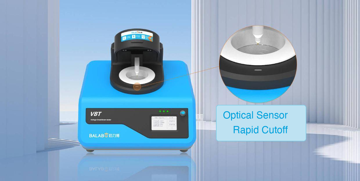
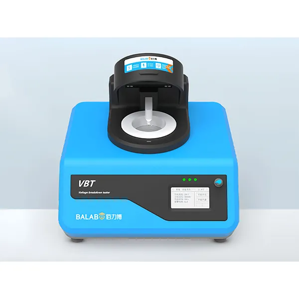
The MatMeas VBT-30KV Voltage Breakdown Tester provides an integrated testing platform engineered specifically to resolve this challenge. Equipped with a digital 30 kV high-voltage supply, the VBT-30KV features a built-in temperature-controlled silicone oil bath capable of operating from ambient room temperature up to +180 C. This allows researchers to suppress parasitic surface flashover while mapping the thermal breakdown curve of technical ceramics and high-voltage polymers across the exact operating temperature range of automotive and aerospace power electronics. Furthermore, because 30 kV breakdown releases substantial explosive plasma energy, the VBT-30KV incorporates an ultrafast optical and electronic trip-relay isolation circuit, clamping output voltage within microseconds of puncture to preserve the ceramic failure channel for post-mortem scanning electron microscopy (SEM) analysis.
Standardized Step-by-Step SOP for Voltage Breakdown Characterization
To achieve reproducible dielectric breakdown data complying with ASTM D149 and IEC 60243-1, testing laboratories should enforce this structured protocol:
Step 1: Specimen Preparation and Dimensional Inspection
- Machine ceramic test specimens as flat discs or square plates. For high-permittivity ceramics, recessed spherical dimples (cavity specimens) may be diamond-ground into the center to reduce local thickness h to 0.2 mm to 0.5 mm, guaranteeing volume puncture at manageable voltages.
- Measure the exact thickness h at the center of the test area using a calibrated micrometer with a spherical anvil (+/-0.001 mm accuracy).
- Ultrasonically clean the specimen in acetone, rinse in isopropanol, and bake at 150 C for 2 hours to eliminate all surface moisture.
Step 2: Electrode Application and Oil Bath Immersion
- Apply thin sputtered gold/platinum electrodes or circular conductive paste contacts. To prevent edge-effect corona discharge, ensure electrodes have smoothly rounded perimeters.
- Mount the specimen between opposing spherical or flat cylindrical brass/stainless steel electrodes complying with ASTM D149 Table 1.
- Submerge the entire fixture assembly into the silicone oil chamber. Allow 15 minutes for oil degassing and thermal equilibrium, ensuring no air bubbles adhere to the ceramic-electrode interface.
Step 3: Voltage Ramping and Mode Selection
- Short-Time (Rapid-Rise) Test: Program the digital high-voltage generator to ramp voltage linearly at a standardized rate of 500 V/s (or 1000 V/s) until puncture occurs. Record the peak breakdown voltage V_b.
- Step-by-Step Withstand Test: For quality control verification, step voltage to 50% of the anticipated breakdown level, holding for 60 seconds. Advance voltage in 1 kV increments, holding for 60 seconds at each plateau to verify steady-state insulation withstand.
Step 4: Weibull Statistical Analysis
- Dielectric breakdown in brittle ceramics is inherently stochastic due to the random spatial distribution of microstructural flaws. Never rely on a single breakdown test.
- Test a minimum cohort of 15 to 20 identical specimens under identical conditions.
- Fit the recorded breakdown fields E_b to a two-parameter Weibull distribution:
P(E_b) = 1 - exp[-(E_b / E_0)^beta]
Where P is the cumulative failure probability, E_0 is the characteristic breakdown strength (corresponding to a 63.2% failure probability), and beta is the Weibull shape parameter (slope). A high beta (beta > 15) indicates uniform microstructural quality and narrow flaw distributions, whereas a low beta (beta < 5) signals erratic manufacturing quality.
Frequently Asked Questions (FAQ)
Why is liquid silicone oil immersion necessary when testing ceramic breakdown voltages?
Air has a dielectric breakdown strength of only ~3 kV/mm. When applying kilovolt voltages to a 1 mm ceramic specimen in air, the electric field ionizes the surrounding air, creating a surface flashover arc across the specimen perimeter. Submerging the specimen in high-dielectric silicone oil (strength > 25 kV/mm) suppresses air ionization and forces the electric field to penetrate the bulk volume of the ceramic.
What is the physical difference between electronic breakdown and thermal breakdown?
Electronic breakdown is an ultrafast (nanosecond) phenomenon caused by impact ionization where high-energy electrons collide with lattice atoms, generating an avalanche plasma channel. Thermal breakdown occurs over milliseconds to seconds when internal Joule heating from electrical conductivity or AC dielectric loss exceeds the rate of heat dissipation, causing localized thermal runaway and melting.
Why do fine-grained ceramics possess higher dielectric strength than coarse-grained ceramics?
Fine-grained ceramics have a vastly higher density of grain boundaries per unit volume. Grain boundaries scatter accelerating conduction electrons, shortening their mean free path and preventing them from acquiring sufficient kinetic energy to initiate impact ionization. Additionally, fine-grained ceramics typically contain smaller sintering pores, which minimizes localized electric field concentration.
How does the VBT-30KV protect internal electronics and operators during high-voltage flashover?
A 30 kV dielectric puncture releases rapid high-frequency transient discharge surges that can destroy electronic controllers. The VBT-30KV integrates a microsecond-response optical and electronic trip sensor that detects current spikes within microseconds, isolating the high-voltage supply through dedicated dump resistors. Operator safety is ensured through a heavy Faraday grounded enclosure and dual-channel mechanical interlocks.
Request High-Precision Testing Solutions
Get expert guidance and customized instruments for your functional materials project.