Advancements in Volume Resistivity Testing for Modern Material Science
Technical News
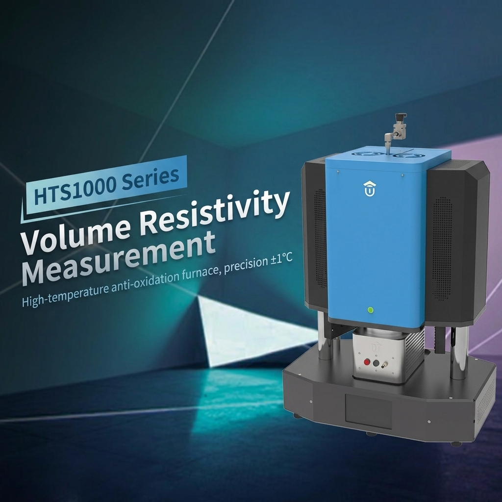
Volume resistivity testing represents one of the most foundational characterization disciplines across modern materials science, physics, and electrical engineering. As an intrinsic property independent of specimen geometric scale, volume resistivity (rho_v) quantifies a material's fundamental ability to oppose or facilitate the transport of electrical charge carriers under an applied electric field. Across modern engineering ecosystems—from power transmission grids and wide-bandgap (WBG) traction inverters to lithium-ion battery electrodes, aerospace composite skins, and nuclear fusion reactor diverters—measuring volume resistivity provides indispensable data for component screening, thermal modeling, and life-cycle reliability qualification.
However, electrical metrology spans an astonishing 25 orders of magnitude in resistivity. At one extreme, highly conductive metallic alloys, superconducting ribbons, and graphite blocks exhibit ultra-low resistivities down to 10^-8 ohmm (10^-6 ohmcm), demanding the measurement of sub-microvolt potentials across milliohm or micro-ohm resistances. At the opposing extreme, technical ceramics, polymer dielectric films, and silica glass substrates display ultra-high resistivities exceeding 10^14 ohmm (10^16 ohmcm), generating minute picoampere or femtoampere currents when subjected to hundreds of volts.
A common failure among testing laboratories is treating volume resistivity testing as a monolithic, one-size-fits-all procedure. Attempting to characterize high-resistance insulators with low-impedance four-point setups, or applying high-voltage two-terminal electrometers to conductive metals, introduces devastating systemic errors. Achieving true metrological traceability requires pairing the material's specific conduction regime with its governing international testing standard—primarily ASTM D257 and IEC 62631-3-1 for high-resistance insulating media, versus ASTM B193, ASTM C611, and SEMI MF84 for low-resistance conductors.
Metrological Paradigms: Insulators vs. Conductors Across Extreme Impedance Domains
To establish rigorous laboratory protocols, test engineers must distinguish between the electrical, mechanical, and thermal constraints governing insulator and conductor characterization. The following matrix illustrates the fundamental dichotomy between these two measurement worlds.
| Metrological Feature | High-Resistance Insulating Materials (Dielectrics) | Low-Resistance Conductive Materials (Metals, Carbon, Oxides) |
|---|---|---|
| Typical Resistivity Span | 10^6 ohmcm to 10^17 ohmcm (Mega-ohm to Peta-ohm regime) | 10^-6 ohmcm to 10^2 ohmcm (Micro-ohm to Ohm regime) |
| Excitation Mode | Constant high-voltage DC source (10 V to 1000 V DC) | Constant high-current DC source (1 mA to 10 A DC) |
| Monitored Electrical Signal | Ultra-weak conduction current (10^-15 A to 10^-9 A, femto to picoamps) | Minute potential drop (10^-8 V to 10^-3 V, nanovolt to millivolt) |
| Dominant Parasitic Error | Surface leakage currents and fixture dielectric shunt dissipation | Lead wire resistance, contact resistance, and Seebeck thermal EMF |
| Standard Electrode Architecture | Guarded three-electrode ring configuration (ASTM D257 / IEC 62631) | Four-terminal Kelvin or collinear four-point probe (ASTM B193 / ASTM C611) |
| Error Cancellation Technique | Active equipotential guard ring shunting surface currents to ground | Bipolar delta-mode current reversal cancelling thermoelectric Seebeck offsets |
| High-Temp Failure Mechanism | Fixture ceramic insulators become conductive, shunting sample current | Specimen oxidizes; thermal gradients generate massive thermoelectric EMF voltages |
| Atmospheric Shielding | Faraday cage electrostatic shielding + high-vacuum/dry nitrogen | Ultra-high purity inert gas (Ar/N2) or high vacuum (< 10^-3 Pa) |
High-Resistance Insulators: ASTM D257 Three-Ring Architecture and Absorption Dynamics
When evaluating solid electrical insulators—such as alumina substrates, piezoelectric ceramics, PTFE polymers, or silicon potting compounds—a simple two-terminal measurement fails catastrophically. The measuring electrometer cannot differentiate between bulk volume current flowing through the material's thickness and surface leakage currents shunting across the specimen's exterior edges due to moisture films and dust.
To resolve this, ASTM D257 and IEC 62631-3-1 mandate the concentric guarded three-electrode architecture:
- Electrode 1 (Guarded Center Electrode): Positioned on the top surface, measuring the pure bulk volume current I_v.
- Electrode 2 (Guard Ring): Concentric with the center electrode on the top surface, separated by an annular gap g. It collects surface leakage current I_s and routes it directly to the virtual-ground terminal of the electrometer, bypassing the measurement ammeter.
- Electrode 3 (Counter Electrode): Covers the entire opposing bottom surface, connected to the high-voltage DC excitation supply.
Under this guarded geometry, the volume resistivity rho_v is derived as:
rho_v = R_v * (A_eff / h) = (V / I_v) * [(pi / 4) * (d1 + g)^2 / h]
Where V is the applied DC test voltage, I_v is the steady-state volume current, h is the specimen thickness, d1 is the diameter of the center electrode, and g is the guard ring gap width.
Furthermore, solid dielectrics do not behave as pure ohmic resistors upon the instantaneous application of a DC voltage. The total current I_total(t) entering the material decays over time according to the classical Curie-von Schweidler law:
I_total(t) = I_geom + I_absorp(t) + I_cond = C * (dV/dt) + A_0 * t^(-n) + (V / R_v)
Where:
- I_geom = C * (dV/dt): The instantaneous geometric capacitive charging current, which decays within milliseconds.
- I_absorp(t) = A_0 * t^(-n): The time-dependent dielectric absorption current resulting from dipole reorientation and interfacial Maxwell-Wagner-Sillars polarization, where the exponent n typically ranges from 0.6 to 1.0.
- I_cond = V / R_v: The true, steady-state ohmic conduction current resulting from intrinsic and extrinsic mobile ions and electronic hopping.
Because absorption current can persist for minutes or hours in high-grade insulators, ASTM D257 mandates a standardized electrification time of exactly 60 seconds (1 minute) before recording current data, guaranteeing reproducible and comparable metrics across global laboratories.
Low-Resistance Conductors: ASTM B193 Four-Terminal Kelvin Metrology and Thermal EMF Cancellation
In stark contrast to insulators, measuring conductive materials such as graphite crucibles, copper-clad laminates, metal alloys, and solid-state battery conductors involves large currents and extremely small voltage drops. Utilizing a standard two-wire setup introduces massive errors because the lead resistance of the test cables (typically 10 mOhm to 100 mOhm) and the contact resistance between probes and sample can exceed the resistance of the specimen itself.
The solution is the Kelvin four-terminal method governed by ASTM B193 (for metallic conductors) and ASTM C611 (for carbon and graphite). The system applies a stable, known DC excitation current I through two outer current electrodes, while two independent high-impedance inner potential sensing probes measure the voltage drop V_x across a calibrated gauge length L:
R_x = V_x / I
rho = R_x * (A / L) = (V_x / I) * (w * t / L)
Where A is the cross-sectional area (width w multiplied by thickness t for rectangular bars, or pi * r^2 for cylindrical rods), and L is the precise distance between the inner voltage sensing probes. Because the voltmeter possesses input impedance in the giga-ohm to tera-ohm range, practically zero current traverses the inner voltage leads, rendering contact resistance and cable lead resistance completely negligible.
The Physics of Dynamic Thermal EMF Cancellation
When conducting high-temperature resistivity tests on conductors up to 1000 C, the most severe source of measurement corruption is the Seebeck thermoelectric effect. Any minute thermal gradient (delta_T) across the sample or between the sample and dissimilar metallic measurement probes (such as tungsten, platinum, or nickel) creates a thermocouple junction. This junction generates a parasitic Seebeck thermoelectric electromotive force (V_Seebeck):
V_Seebeck = integral(S_probe(T) - S_sample(T)) dT
In micro-ohm resistance measurements where the true IR drop V_x is merely a few microvolts, an uncompensated thermal EMF of 50 uV to 500 uV can completely swamp the signal, often causing multimeters to display negative resistance readings.
To eliminate thermal EMF, modern precision systems deploy bipolar delta-mode current reversal. The instrument delivers a rapid sequence of alternating forward (+I) and reverse (-I) current pulses:
V_forward = (+I) * R_x + V_Seebeck
V_reverse = (-I) * R_x + V_Seebeck
Subtracting the two voltage measurements completely eliminates the common-mode thermal EMF offset:
V_true = (V_forward - V_reverse) / 2 = I * R_x
R_x = (V_forward - V_reverse) / (2 * I)
Simultaneously, the true Seebeck thermal EMF can be tracked dynamically:
V_Seebeck = (V_forward + V_reverse) / 2
This mathematical cancellation ensures that sub-micro-ohm volume resistivity data remains pristine even inside high-gradient furnace hot zones.
Benchmark Comparison Across Functional Materials Classes
The following benchmark table illustrates the vast operational spectrum of volume resistivity, corresponding testing architectures, and thermal limits across major materials classes.
| Material Classification | Representative Chemistry / Grade | Room-Temp Volume Resistivity rho_v (ohm*cm) | High-Temp Resistivity at 800 C (ohm*cm) | Primary Conduction Mechanism | Dominant Test Standard | Optimal Testing Fixture Architecture |
|---|---|---|---|---|---|---|
| High-Conductivity Metal | Pure Copper (C11000 / ETP) | 1.72 * 10^-6 | 7.5 * 10^-6 | Free electron gas; lattice phonon scattering | ASTM B193 | 4-terminal Kelvin; bipolar current reversal; vacuum chamber |
| Industrial Carbon / Graphite | Nuclear-grade Isotropic Graphite | 1.1 * 10^-3 | 1.3 * 10^-3 | Semi-metallic pi-electrons; boundary scattering | ASTM C611 | 4-terminal bar geometry; dynamic Seebeck cancellation |
| High-Temp Semiconducting Oxide | Sintered Silicon Carbide (SiC) | 1.0 * 10^1 to 10^3 | 1.0 * 10^-1 to 10^1 | Thermally activated polarons; band hopping | SEMI MF84 | Collinear 4-point probe; high-temp platinum pressure contacts |
| Thermal Dissipation Substrate | Aluminum Nitride (AlN) Ceramic | 1.0 * 10^14 | 2.0 * 10^7 | Extrinsic vacancy migration; defect hopping | ASTM D257 | Guarded 3-ring platinum electrode; corundum insulation |
| High-Purity Technical Ceramic | 99.8% Alumina (alpha-Al2O3) | 5.0 * 10^15 | 8.0 * 10^8 | Doubly ionized oxygen vacancy hopping | ASTM D257 | Guarded 3-ring sapphire isolated stage; 0.25 N micro-load |
| Refractory Oxide Glass | Fused Silica (SiO2) Glass | > 1.0 * 10^17 | 1.0 * 10^9 | Pure ionic migration (alkali trace impurities) | IEC 62631 | Ultra-high temperature 3-terminal guarded muffle furnace |
Dedicated Instrumentation: HTS-1000HR, RTS-1000C, and RMS-1650
Because the physical requirements for insulating and conductive materials are completely divergent, MatMeas provides dedicated hardware platforms tailored specifically to each impedance extreme:
For ultra-high-resistance insulators, the MatMeas HTS-1000HR High Temperature Resistivity Measurement System is engineered specifically for materials spanning 10^3 ohm to 10^15 ohm up to +800 C. The HTS-1000HR features high-purity recrystallized alumina and sapphire insulation stacks that prevent fixture leakage from corrupting picoampere signals. Utilizing a factory-calibrated maximum clamping load of just 0.25 N, the system prevents mechanical micro-cracking in fragile ceramic substrates and thin dielectric discs while providing sealed vacuum and inert gas shielding against platinum electrode oxidation.
Conversely, for low-resistance conductors, graphite, and functional semiconductors spanning 10 nΩ to 100 MΩ under elevated temperatures, the MatMeas RTS-1000C High-Temp Conductive Material Resistivity System (the upgraded evolution of the earlier RMS-1000C platform) deploys a four-terminal Kelvin configuration driven by high-speed bipolar current reversal. Incorporating dense 99% Zirconia (ZrO₂) thermal isolation and hybrid platinum/tungsten-carbide probes, the system mathematically cancels out Seebeck thermoelectric EMF voltages in real time. Operating within a sealed vacuum/inert atmosphere chamber, the RTS-1000C prevents oxidation of sensitive graphite, metal alloys, and functional conductive oxides.
For ultra-extreme thermal regimes beyond 1000 C, the MatMeas RMS-1650 Ultra-High Temperature Resistivity Measurement System extends characterization capabilities up to +1600 C. Housed within a shielded corundum muffle chamber with platinum-rhodium electrodes, the RMS-1650 utilizes active three-terminal guarding to isolate bulk volume resistivity from massive surface ionic leakage currents under extreme thermal stress.
Standardized Step-by-Step SOP for Volume Resistivity Testing
Achieving repeatable, publication-grade volume resistivity data requires executing this standardized laboratory protocol:
Step 1: Material Categorization and Method Selection
- Perform a rough two-point preliminary screening with a handheld digital multimeter.
- If resistance R > 10^7 ohm, classify the sample as an insulator and select the ASTM D257 guarded three-electrode method.
- If resistance R < 10^4 ohm, classify the sample as a conductor and select the ASTM B193 or ASTM C611 four-terminal Kelvin method.
Step 2: Specimen Geometry and Surface Preparation
- For insulators, prepare uniform flat discs or square plates (thickness h between 0.5 mm and 2.0 mm; faces parallel within +/-0.01 mm). Polish surfaces to eliminate conductive contamination. Clean ultrasonically in acetone and bake at 120 C for 30 minutes.
- For conductors, machine uniform rectangular bars or cylindrical rods with a high length-to-cross-section aspect ratio (L / sqrt(A) >= 5) to ensure parallel current flow lines between inner potential taps.
Step 3: Fixture Installation and Thermal Shielding
- For insulators, install the specimen inside the shielded three-electrode fixture. Ensure the guard ring is connected directly to the electrometer guard shield. Apply a gentle contact load (0.25 N for fragile ceramics).
- For conductors, clamp the outer current leads and mount spring-loaded knife-edge potential probes at calibrated distance L. Verify firm mechanical contact without surface indentation.
- Seal the environmental test chamber and evacuate to high vacuum (< 10^-2 Pa) or backfill with high-purity argon (99.999%) to protect both sample and electrodes during heating.
Step 4: Measurement Execution and Thermal Profiling
- For insulators: Apply test voltage (100 V DC or 500 V DC). Wait exactly 60 seconds of electrification time before logging the volume current I_v.
- For conductors: Initiate bipolar current pulsing (+I, -I). Confirm that the delta-mode algorithm successfully nulls the Seebeck thermal EMF.
- Initiate the thermal cycle at a steady ramp rate (recommended: 2 C/min to 5 C/min). Log discrete resistance data at specified temperature intervals during both heating and cooling cycles to identify any thermal hysteresis or irreversible microstructural changes.
Frequently Asked Questions (FAQ)
Why can't a single universal instrument measure both conductors and insulators accurately?
Conductors and insulators occupy opposite extremes of electrical impedance. Testing a conductor requires sourcing up to several amperes of current and measuring nanovolts, where contact resistance and Seebeck thermal EMF dominate errors. Testing an insulator requires sourcing hundreds of volts and measuring femtoamperes, where surface leakage and fixture insulation breakdown dominate errors. Hardware architectures optimized for one extreme are fundamentally incapable of resolving the other.
How does Seebeck thermal EMF distort high-temperature conductor measurements?
When a conductive specimen is heated in a furnace, thermal gradients exist across the sample. The physical junctions between the sample and the measurement probes act as thermocouples, generating a DC voltage (often tens to hundreds of microvolts). In low-resistance measurements where the actual IR drop is only a few microvolts, this thermoelectric voltage will cause massive errors or even produce negative resistance values unless bipolar current reversal is employed.
Why is an active guard ring essential when measuring high-resistance ceramics?
At room temperature and high relative humidity, thin moisture films and dust on ceramic surfaces create surface leakage paths with resistances far lower than the true bulk volume resistance. A simple two-electrode test measures volume and surface resistance in parallel, resulting in a drastically false low reading. The ASTM D257 guard ring captures surface current and shunts it safely to ground, ensuring the picoammeter measures strictly the internal volume conduction.
How does atmospheric control protect electrode contacts at elevated temperatures?
Exposing test fixtures to ambient air above 400 C causes rapid oxidation of metallic electrodes (such as copper, nickel, or silver) and burns carbon/graphite specimens into carbon dioxide gas. Operating within a sealed chamber supporting high vacuum or high-purity inert argon prevents oxidation, maintains stable metal-ceramic interfacial contact, and prevents electrical flashover ionization at elevated voltages.
Related Instruments & Equipment
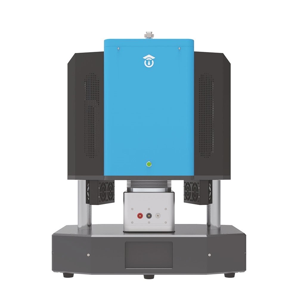
HTS1000HR High Temperature Resistivity Measurement System
The HTS1000HR is an advanced, integrated testing platform specifically engineered to precisely evaluate the electrical conductivity and insulation properties of advanced materials at extreme temperatures up to 800℃. By supporting various atmospheric conditions and offering an ultra-wide resistance measurement range, it serves as an indispensable characterization tool for material research and industrial quality control.
View details →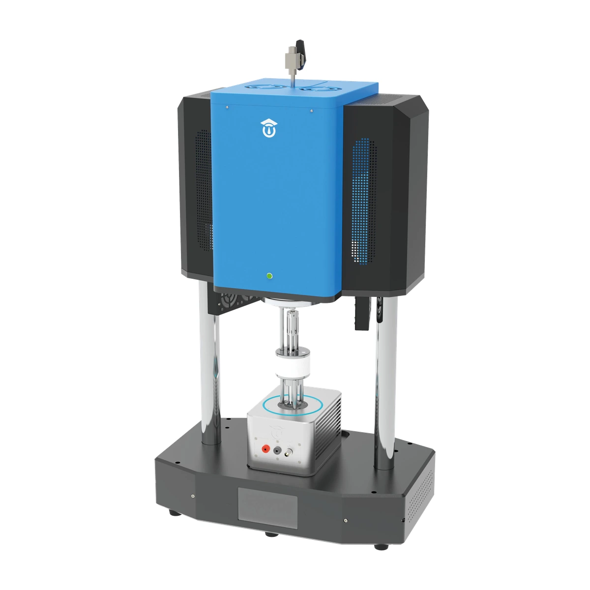
MatMeas RTS-1000C High-Temp Conductive Material Resistivity System (Upgraded from RMS-1000C)
The MatMeas RTS-1000C is the next-generation flagship evolution of the earlier RMS-1000C system, purpose-built for precision high-temperature conductive material resistivity measurement via four-wire Kelvin method. Delivering nΩ-to-MΩ resolution (10 nΩ to 100 MΩ) from RT to 600°C (±1°C PID), the upgraded platform features 99% zirconia thermal isolation, a rigid motorized test stand, and hybrid platinum/tungsten-carbide probes for vacuum and controlled atmospheres.
View details →
RMS1650 Ultra-High Temperature Resistivity Measurement System
The RMS1650 Ultra-High Temperature Resistivity Measurement System is engineered for the rigorous electrical characterization of insulating and dielectric materials up to 1600°C. Utilizing a proprietary guarded three-terminal electrode configuration, the system enables in-situ acquisition of resistivity and leakage current kinetics under extreme temperatures, vacuum, and controlled gas atmospheres.
View details →Request High-Precision Testing Solutions
Get expert guidance and customized instruments for your functional materials project.