Ceramic Substrate Resistivity Testing Technology and Application Analysis
Technical News

Advanced ceramic substrates serve as the foundational thermal and electrical isolation backbone for modern wide-bandgap (WBG) power semiconductors, insulated gate bipolar transistor (IGBT) modules, automotive traction inverters, aerospace motor drives, and radio-frequency (RF) radar packages. Materials such as high-purity alumina (Al2O3), aluminum nitride (AlN), silicon nitride (Si3N4), and low-temperature co-fired ceramics (LTCC) are uniquely positioned to meet these punishing operating regimes. They simultaneously deliver high mechanical stiffness, superior thermal conductivity, excellent chemical inertness, and near-flawless dielectric isolation.
In high-voltage power conversion modules—where continuous bus voltages exceed 1.2 kV, 3.3 kV, or even 10 kV in next-generation silicon carbide (SiC) and gallium nitride (GaN) systems—the electrical resistivity of the underlying ceramic baseplate is the ultimate metric governing system reliability. If volume or surface resistivity degrades under operational thermal cycles, parasitic leakage currents escalate exponentially. This parasitic conduction leads to localized ohmic self-heating, thermal runaway, premature dielectric puncture, and catastrophic short-circuit failure.
Evaluating both volume resistivity (rho_v) and surface resistivity (rho_s) across an extended temperature envelope—from ambient room temperature up to +800 C or +1600 C—is therefore not merely a materials characterization exercise, but a life-cycle qualification requirement regulated by ASTM D257, IEC 62631-3-1, and SEMI G44.
Fundamental Definitions and Governing Physical Equations
Electrical resistivity in solid dielectric ceramics is fundamentally divided into two distinct current conduction pathways: bulk volume conduction through the polycrystalline grains and grain boundaries, and superficial surface conduction driven by adsorbed moisture, ambient contaminants, and interfacial termination states.
1. ASTM D257 Volume Resistivity Formulation
Volume resistivity (rho_v) characterizes the intrinsic capability of the bulk ceramic material to impede electrical current flowing perpendicularly through its thickness h. Under the guarded three-electrode test configuration defined by ASTM D257 and IEC 62631-3-1, an applied direct-current (DC) potential V produces a steady-state volume current I_v through the center guarded electrode. The volume resistivity is calculated as:
rho_v = R_v * (A_eff / h)
Where:
- R_v: The measured bulk volume insulation resistance in ohms (R_v = V / I_v).
- h: The average thickness of the ceramic substrate specimen in centimeters or meters.
- A_eff: The effective area of the central measuring electrode, incorporating an edge-field fringe correction across the annular guard gap:
A_eff = (pi / 4) * (d1 + g)^2
Where d1 represents the outer diameter of the guarded circular measuring electrode, and g denotes the radial air gap width separating the center electrode from the concentric guard ring. This geometric fringe formulation assumes that the electric field lines traverse uniformly through the ceramic volume, splitting evenly along the centerline of the guard gap.
2. ASTM D257 Surface Resistivity Formulation
Surface resistivity (rho_s) represents the electrical resistance to leakage current flowing across a unit square of the ceramic substrate surface. Measured across the annular guard gap g between the guarded center electrode and the outer guard ring under a DC test potential V, the surface leakage current I_s yields the surface resistance R_s (R_s = V / I_s). The normalized surface resistivity is expressed in ohms per square (ohm/sq):
rho_s = R_s * (P_eff / g) = R_s * [pi * (d1 + g) / g]
Where P_eff = pi * (d1 + g) is the effective circumference along the midpoint of the annular guard gap. Surface resistivity is exquisitely sensitive to atmospheric humidity, surface roughness, grain boundary oxidation, and chemical residues from thick-film metallization or direct bonded copper (DBC) etching processes.
Thermal Activation and Arrhenius Ionic Conduction Dynamics
At room temperature (25 C), high-quality technical ceramics behave as near-perfect insulators, with volume resistivities frequently exceeding 10^14 ohmcm to 10^16 ohmcm. In this regime, intrinsic free electron and hole concentrations are negligible due to wide bandgaps (9.0 eV for Al2O3, 6.2 eV for AlN, and 5.1 eV for Si3N4). Conduction is dominated by extrinsic defect states and trace impurities.
However, as operating temperatures rise past 200 C and into the 600 C to 1000 C domain, thermally activated ionic migration and polaron hopping become the dominant conduction mechanisms. Point defects—most notably doubly ionized oxygen vacancies (V_O_ddot) in oxide ceramics or nitrogen vacancies and aluminum interstitials in nitride matrices—gain sufficient thermal energy to jump over crystalline energy barriers.
This temperature dependence follows the classic Arrhenius conduction law:
sigma(T) = sigma_0 * exp(-E_a / (k_B * T))
Converting conductivity sigma(T) to volume resistivity rho_v(T) yields:
rho_v(T) = rho_0 * exp(E_a / (k_B * T))
Where:
- sigma_0 and rho_0: The pre-exponential material constants determined by carrier mobility and defect concentration.
- E_a: The thermal activation energy for electrical transport (typically 0.8 eV to 1.6 eV for alumina and aluminum nitride).
- k_B: The Boltzmann constant (8.617 * 10^-5 eV/K).
- T: The absolute temperature in Kelvin (K).
Because of this exponential relationship, an increase in operating temperature from 25 C to 500 C causes the volume resistivity of an Al2O3 or AlN substrate to plummet by five to seven orders of magnitude. A substrate measuring 10^14 ohmcm at ambient room temperature may drop to less than 10^8 ohmcm at 600 C. If power module designers do not account for this exponential thermal collapse, high-temperature switching transients will trigger catastrophic localized breakdown.
Material Benchmark Comparison: Technical Ceramics for Power Electronics
Selecting the optimum ceramic substrate for high-voltage power electronics requires balancing volume resistivity, dielectric withstand strength, thermal conductivity, and mechanical fracture toughness. The following table provides a comprehensive benchmark of leading ceramic substrate formulations.
| Ceramic Substrate Material | Typical Purity / Composition | Room-Temp Volume Resistivity rho_v (ohm*cm) | 500 C Volume Resistivity rho_v (ohm*cm) | Surface Resistivity rho_s at 25 C (ohm/sq) | Thermal Conductivity kappa (W/m*K) | Dielectric Breakdown Strength (kV/mm) | CTE (ppm/K, 25 C to 400 C) | Primary Electronic Packaging Application Envelope |
|---|---|---|---|---|---|---|---|---|
| Alumina 96% (Al2O3) | 96% Al2O3 + SiO2/MgO fluxes | 1.0 * 10^14 | 2.5 * 10^8 | 5.0 * 10^13 | 24 to 28 | 15 to 18 | 7.1 | Cost-sensitive automotive ECUs, industrial power supplies, thick-film hybrids |
| High-Purity Alumina 99.6% | 99.6% alpha-Al2O3 (thin-film) | 5.0 * 10^15 | 8.0 * 10^9 | 1.0 * 10^15 | 32 to 36 | 20 to 25 | 7.4 | Thin-film microwave integrated circuits (MICs), laser submounts, photodetectors |
| Aluminum Nitride (AlN) | >99% AlN + Y2O3 sintering aid | 1.0 * 10^14 | 1.2 * 10^8 | 2.0 * 10^13 | 170 to 220 | 18 to 22 | 4.6 | High-heat-flux traction inverters, wind turbine IGBTs, laser diode heat spreaders |
| Silicon Nitride (Si3N4) | beta-Si3N4 (gas-pressure sintered) | 5.0 * 10^13 | 5.0 * 10^7 | 8.0 * 10^12 | 80 to 90 | 25 to 30 | 3.2 | High-reliability electric vehicle (EV) inverters, extreme thermal shock modules |
| Beryllia (BeO) | 99.5% BeO (toxic handling) | 1.0 * 10^15 | 3.0 * 10^9 | 5.0 * 10^14 | 250 to 280 | 12 to 15 | 8.0 | Military high-power RF transmitters, high-frequency traveling-wave tubes |
| LTCC Glass-Ceramic | Crystallized borosilicate glass | 1.0 * 10^13 | 1.0 * 10^7 | 1.0 * 10^12 | 2 to 5 | 12 to 16 | 5.8 | Multilayer RF radar modules, 5G transceiver front-ends, aerospace avionics |
Guarded Three-Electrode Metrology vs. Conventional Two-Terminal Testing
Accurately measuring ultra-high resistances (10^12 ohm to 10^16 ohm) represents one of the most formidable challenges in precision electrical metrology. In a basic two-electrode configuration, surface leakage currents flowing across the exterior edges of the substrate enter the measurement electrometer in parallel with the bulk volume current. Because surface resistivity is often several orders of magnitude lower than volume resistivity due to atmospheric humidity, a two-terminal measurement will drastically underestimate the true bulk insulation resistance.
The guarded three-electrode architecture mandated by ASTM D257 solves this issue by deploying an active guard ring concentric with the center measuring electrode on the top surface, while a solid counter-electrode covers the opposing bottom surface. The guard ring is tied directly to the virtual-ground guard terminal of the electrometer. Consequently, all parasitic surface currents are safely shunted directly to ground without passing through the sensitive picoammeter circuit.
| Metrological Feature | Conventional Two-Electrode Test Fixture | ASTM D257 Guarded Three-Electrode System |
|---|---|---|
| Current Separation | Merges bulk volume and surface leakage currents indiscriminately | Strictly decouples pure bulk volume current (I_v) from surface leakage (I_s) |
| Surface Leakage Shunting | None; surface currents introduce severe false low-resistance errors | Active guard ring shunts surface current to ground via low-impedance bypass |
| Fringe Field Distribution | Non-uniform edge fringing distorts effective electrode geometry | Equipotential guard boundary maintains strictly parallel electric field lines |
| Maximum Measurable Limit | Typically capped at ~10^11 ohm due to stray fixture leakage paths | Resolves up to 10^16 ohm using shielded coaxial triaxial routing |
| Electrification Dynamics | Cannot isolate dielectric polarization currents from surface drift | Accurately records Curie-von Schweidler absorption current decay I(t) proportional to t^(-n) |
| Elevated Temperature Accuracy | Fixture ceramic breakdown creates parallel shunts above 300 C | Specialized sapphire or 99.8% corundum guard isolators operate up to 800 C / 1600 C |
| International Standards Compliance | Non-compliant with ASTM D257, IEC 62631-3-1, and SEMI G44 | Fully compliant with ASTM D257, IEC 62631-3-1, and MIL-I-10 |
High-Temperature Instrumentation Platforms: HTS-1000HR and RMS-1650
Executing ceramic substrate resistivity testing up to 800 C or 1600 C requires specialized mechanical fixtures and environmental containment chambers. At extreme temperatures, standard stainless steel electrodes oxidize rapidly, while generic quartz and ceramic insulation fixtures undergo dielectric breakdown, forming conductive parallel paths that overwhelm the high-resistance substrate under test.
To resolve these high-temperature limitations, the MatMeas HTS-1000HR High Temperature Resistivity Measurement System utilizes an ultra-pure sapphire and 99.8% recrystallized alumina insulation stack. Operating across a temperature span from ambient up to +800 C, the HTS-1000HR features a three-ring platinum electrode fixture driven by a motorized micro-loading stage. The stage applies a calibrated normal force of just 0.25 N, ensuring intimate electrical contact without micro-cracking fragile 0.25 mm to 0.635 mm ceramic substrates. The chamber supports vacuum levels down to 10^-3 Pa, as well as inert argon and nitrogen atmospheres, preventing electrode oxidation and eliminating parasitic air ionization currents.
For ultra-refractory technical ceramics, nuclear reactor insulators, and structural furnace linings operating beyond 1000 C, the MatMeas RMS-1650 Ultra-High Temperature Resistivity Measurement System extends characterization capabilities up to +1600 C. The RMS-1650 deploys platinum-rhodium (Pt-Rh) electrodes housed within a hermetically sealed, water-cooled double-wall vacuum chamber with molybdenum disilicide (MoSi2) heating elements. By integrating high-temperature triaxial guard shielding directly into the hot zone, the RMS-1650 suppresses parasitic furnace leakage, allowing researchers to extract bulk volume resistivity data up to 1600 C.
Step-by-Step SOP for Ceramic Substrate Resistivity Testing
To ensure reproducible measurement data adhering to ASTM D257 and IEC 62631-3-1, testing laboratories must enforce this standardized operating protocol:
Step 1: Specimen Preparation and Cleaning
- Ensure the ceramic substrate is fabricated with flat, parallel faces (parallelism tolerance within +/-0.005 mm). Recommended sample dimensions are 50 mm x 50 mm square or 50 mm diameter discs with thickness h between 0.3 mm and 1.0 mm.
- Subject the specimen to ultrasonic cleaning in high-purity acetone for 10 minutes, followed by 10 minutes in electronic-grade isopropanol.
- Bake the substrate in a clean drying oven at 150 C for at least 60 minutes to eliminate all adsorbed surface moisture films, then transfer immediately to a desiccator to cool.
Step 2: Electrode Metallization
- Apply thin-film platinum or gold electrodes via magnetron sputtering using a precision shadow mask matching ASTM D257 geometry (center electrode diameter d1 = 25.0 mm; guard ring inner diameter d2 = 27.0 mm, yielding an annular gap g = 1.0 mm; counter-electrode diameter d3 >= 35.0 mm).
- Alternatively, for rapid screening, apply high-purity conductive silver paste and fire at 650 C in air according to the paste manufacturer's thermal profile.
Step 3: Fixture Installation and Shielding
- Mount the metallized ceramic substrate onto the bottom counter-electrode stage.
- Carefully lower the upper guarded electrode assembly. Adjust the motorized contact mechanism until a calibrated contact force of 0.25 N to 0.50 N is achieved.
- Secure the Faraday cage enclosure and connect low-noise triaxial cables to the electrometer. Ensure the outer guard shield is connected directly to the electrometer guard terminal.
Step 4: Electrification and Data Acquisition
- Apply the specified DC test voltage (standard: 100 V DC or 500 V DC).
- Monitor current decay over time. In accordance with ASTM D257, allow an electrification time of exactly 60 seconds before logging the final volume current I_v and surface current I_s. This 60-second delay allows dielectric absorption and polarization currents to decay, leaving the true steady-state ohmic conduction current.
- For temperature-dependent profiling, establish an automated thermal ramp rate of 2 C/min to 5 C/min, taking discrete steady-state current measurements at 50 C temperature intervals up to the target maximum temperature.
Frequently Asked Questions (FAQ)
Why is the guarded three-electrode method required instead of a standard two-probe digital multimeter?
Standard digital multimeters and two-probe fixtures cannot measure resistances exceeding 10^9 ohm to 10^10 ohm. Furthermore, a two-probe setup merges bulk volume currents with surface leakage currents flowing across the edges of the substrate. The ASTM D257 guarded three-electrode method deploys an active guard ring that shunts surface currents directly to ground, allowing the electrometer to isolate pure bulk volume currents up to 10^16 ohm*cm.
What is the purpose of the mandatory 60-second electrification time in ASTM D257?
When a DC step voltage is applied across a dielectric ceramic, the initial current consists of instantaneous geometric charging current plus a time-dependent dielectric absorption current governed by the Curie-von Schweidler law: I(t) is proportional to t^(-n). At t = 60 seconds, the absorption current has decayed sufficiently so that the remaining current is dominated by genuine steady-state ohmic conduction.
How does high temperature cause ceramic substrate resistivity to collapse?
Pure electronic ceramic lattices have wide bandgaps (5 eV to 9 eV), meaning thermal energy at room temperature cannot excite electrons across the gap. However, at temperatures above 300 C to 500 C, intrinsic point defects (such as ionized oxygen vacancies V_O_ddot) gain sufficient thermal energy to hop across crystalline lattice barriers. This Arrhenius ionic hopping causes resistivity to decrease exponentially with temperature.
How does the HTS-1000HR prevent delicate ceramic substrates from cracking during testing?
Ceramic substrates for power electronics are often fragile and thin (0.25 mm to 0.635 mm). Heavy mechanical clamping can cause micro-cracks or catastrophic shattering. The HTS-1000HR incorporates a motorized micro-loading mechanism with real-time load cell feedback, applying a controlled contact force of just 0.25 N. This ensures intimate electrical contact with platinum electrodes without risking mechanical damage to the substrate.
Related Instruments & Equipment
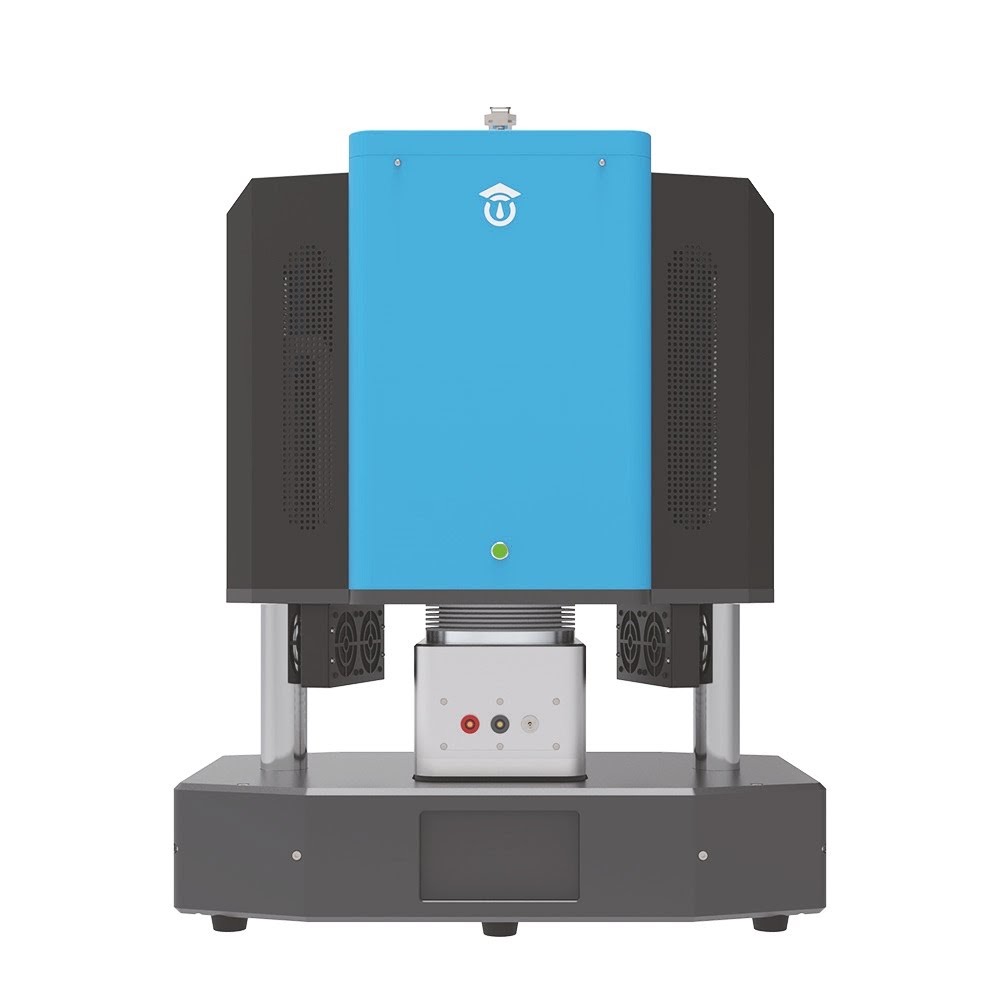
HTS1000HR High Temperature Resistivity Measurement System
The HTS1000HR is an advanced, integrated testing platform specifically engineered to precisely evaluate the electrical conductivity and insulation properties of advanced materials at extreme temperatures up to 800℃. By supporting various atmospheric conditions and offering an ultra-wide resistance measurement range, it serves as an indispensable characterization tool for material research and industrial quality control.
View details →
RMS1650 Ultra-High Temperature Resistivity Measurement System
The RMS1650 Ultra-High Temperature Resistivity Measurement System is engineered for the rigorous electrical characterization of insulating and dielectric materials up to 1600°C. Utilizing a proprietary guarded three-terminal electrode configuration, the system enables in-situ acquisition of resistivity and leakage current kinetics under extreme temperatures, vacuum, and controlled gas atmospheres.
View details →Request High-Precision Testing Solutions
Get expert guidance and customized instruments for your functional materials project.