Four-Point Probe Testing of Graphite Conductivity: Standards, Geometry, and Anisotropy
Technical News
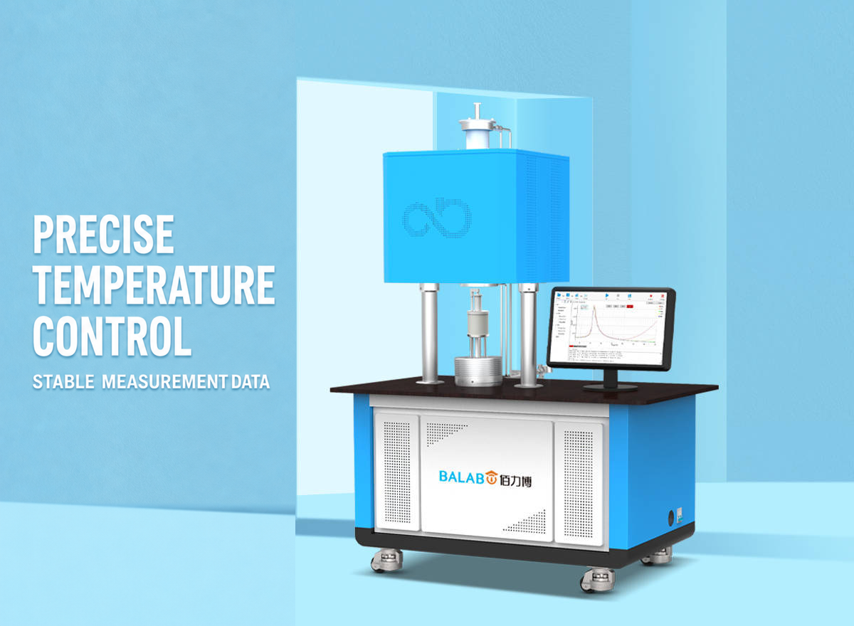
Graphite and carbon-based allotropes occupy an irreplaceable role across high-technology industries. Serving as electric arc furnace electrodes, electrical discharge machining (EDM) dies, nuclear fission moderator blocks, lithium-ion battery anode current collectors, fuel cell bipolar plates, and thermal spreaders for 5G smartphones, graphite's electrical performance dictates device efficiency.
The electrical resistivity (rho) and its reciprocal, electrical conductivity (sigma = 1 / rho), are the primary physical properties governing ohmic power loss, Joule self-heating, and electromigration resistance in graphite components. However, accurately measuring the electrical resistivity of graphite presents unique challenges:
- Severe Electrical Anisotropy: The hexagonal crystalline lattice of graphite yields in-plane conductivities that exceed through-thickness conductivities by up to four orders of magnitude.
- Contact Resistance and Lead Parasitics: Because graphite is a low-resistance conductor (bulk resistivities typically range from 10^-6 ohmm to 10^-4 ohmm), conventional two-probe multimeter methods are dominated by contact resistance and cable impedance.
- Geometric Current Spreading: In thin graphite foils or finite machined blocks, electrical current lines do not propagate through an infinite half-space, demanding rigorous mathematical geometric correction.
The collinear four-point probe method—standardized globally under ASTM F84, SEMI MF84, and ISO 3915—is the definitive metrological solution for evaluating sheet resistance and bulk resistivity in conductive carbonaceous materials.
The Crystallographic Origin of Anisotropic Conduction in Graphite
To correctly interpret four-point probe measurements, test engineers must understand the underlying solid-state physics of the carbon lattice. In an ideal hexagonal graphite crystal (space group P6_3/mmc), carbon atoms are arranged in planar, two-dimensional honeycomb sheets:
- In-Plane (a-b Plane, Basal Plane): Carbon atoms are covalently bonded via strong sp2 hybridized sigma bonds (interatomic distance ~0.142 nm). The remaining unhybridized p_z atomic orbitals overlap laterally to form a delocalized pi-conduction band. In pure single-crystal graphite or Highly Oriented Pyrolytic Graphite (HOPG), electrons and holes exhibit high mean free paths along this plane, yielding in-plane resistivities as low as 4.0 * 10^-5 ohm*cm (conductivity ~2.5 * 10^4 S/cm).
- Out-of-Plane (c-Axis, Transverse Direction): Adjacent graphene basal planes are separated by a relatively wide distance (~0.335 nm) and held together solely by weak van der Waals interactions. Interlayer charge transport requires quantum mechanical tunneling or hopping across this potential barrier. Consequently, c-axis resistivity reaches 0.1 ohmcm to 1.0 ohmcm.
The resulting intrinsic electrical anisotropy ratio (rho_c / rho_ab) can reach 10^3 to 10^4 in highly oriented pyrolytic graphite. While commercial extruded or isostatically molded graphite grades are polycrystalline aggregates, preferential alignment of anisotropic grains during extrusion or pressing induces significant macroscopic anisotropy. A four-point probe placed parallel to the extrusion axis will record a noticeably lower resistivity than when oriented perpendicularly across the pressing axis.
Operating Principle and Mathematical Equations of the Four-Point Probe
The collinear four-point probe configuration deploys four equally spaced, spring-loaded metallic needles in a straight line along the specimen surface:
- Outer Probes (Probe 1 and Probe 4): Inject a regulated direct-current (DC) excitation I from a precision constant-current source.
- Inner Probes (Probe 2 and Probe 3): Sense the resulting electrostatic potential drop delta_V across the material using an electrometer with input impedance exceeding 10^12 ohms.
Because the potential-sensing circuit draws virtually zero current, no voltage drop occurs across the contact resistance at the probe-sample interface or within the test leads. This completely eliminates contact resistance from the measurement equation.
1. Semi-Infinite Bulk Medium (Three-Dimensional Current Spherical Spreading)
When the graphite specimen is semi-infinite in all directions—meaning its thickness t and lateral dimensions w are substantially greater than the probe spacing s (typically t >= 5 * s)—current spreads spherically from Probe 1 and converges into Probe 4. Integrating the potential field across the semi-infinite hemisphere yields:
rho_bulk = 2 * pi * s * (delta_V / I)
Where:
- s: The uniform spacing between adjacent probes (typically s = 1.0 mm or 1.588 mm).
- delta_V: The measured voltage drop between Probe 2 and Probe 3 (volts).
- I: The applied DC excitation current (amperes).
2. Thin Sheets and Foils: The Smits Thickness Correction Formulation
When measuring thin graphite foils, flexible exfoliated graphite sheets, or thin pyrolytic films where thickness t is much smaller than probe spacing s (t <= 0.5 * s), current is constrained to spread as cylindrical rings in two dimensions. Under this boundary condition, sheet resistance R_sq (expressed in ohms per square, ohm/sq) is calculated as:
R_sq = (pi / ln 2) * (delta_V / I) approx 4.53236 * (delta_V / I)
The three-dimensional volume resistivity rho is then derived by multiplying sheet resistance by the actual specimen thickness t and the Smits geometric correction factor F(t / s):
rho = R_sq * t * F(t / s) = 4.53236 * (delta_V / I) * t * F(t / s)
Where F(t / s) is the classical Smits thickness correction function governed by ASTM F84 and SEMI MF84:
F(t / s) = (t / s) / [ (2 * ln 2 / pi) * sum_n=1^infinity [ 1 / sqrt((t/s)^2 + (n - 1/2)^2) - 1 / sqrt((t/s)^2 + n^2) ] ]
When t / s <= 0.5, the correction factor F(t / s) approaches 1.000 with less than 0.1% error. However, when sample thickness lies in the transitional intermediate regime (0.5 < t / s < 5.0), failing to apply F(t / s) introduces severe measurement errors exceeding 10% to 50%.
Smits Thickness Correction Factors and Current Spreading Regimes
The following table provides verified Smits correction factors F(t / s) and current spreading characteristics across varying thickness-to-spacing ratios.
| Thickness-to-Spacing Ratio (t / s) | Smits Correction Factor F(t / s) | Current Spreading Regime | Error if Thin-Sheet Formula Used Directly | Representative Graphite Specimen Geometry |
|---|---|---|---|---|
| t / s = 0.10 | 1.0000 | Pure two-dimensional (cylindrical) | < 0.01% (Negligible) | 100 um flexible exfoliated graphite foil, graphene paper |
| t / s = 0.20 | 1.0000 | Strictly two-dimensional | < 0.05% | 200 um pyrolytic graphite heat-spreading film |
| t / s = 0.40 | 0.9995 | Weak three-dimensional fringing | 0.05% | 400 um battery anode graphite current collector |
| t / s = 0.50 | 0.9974 | Transition boundary onset | 0.26% | 0.5 mm fuel cell graphite composite bipolar plate |
| t / s = 0.70 | 0.9787 | Intermediate 2D/3D mixed spreading | 2.13% | 0.7 mm thin-sliced EDM graphite wafer |
| t / s = 1.00 | 0.9214 | Moderate three-dimensional divergence | 7.86% | 1.0 mm machined nuclear graphite test disc |
| t / s = 1.50 | 0.7879 | Strong three-dimensional divergence | 21.21% | 1.5 mm structural graphite plate |
| t / s = 2.00 | 0.6336 | Severe three-dimensional divergence | 36.64% | 2.0 mm graphite block coupon (approaching bulk) |
| t / s >= 5.00 | Requires 2 * pi * s bulk formula | Pure three-dimensional (spherical) | Invalid (must use semi-infinite equation) | Massive EDM graphite block, nuclear core brick |
Anisotropic Material Benchmarks Across Graphite Classes
The following benchmark table compares the directional electrical resistivity, anisotropy ratio, and thermal properties across leading industrial, nuclear, and pyrolytic graphite formulations.
| Graphite Material Grade | Microstructural Classification | In-Plane Resistivity rho_ab (ohm*cm) | Out-of-Plane Resistivity rho_c (ohm*cm) | Anisotropy Ratio (rho_c / rho_ab) | Thermal Conductivity (W/m*K) | Bulk Density (g/cm3) | Primary Industrial / Scientific Application |
|---|---|---|---|---|---|---|---|
| HOPG (ZYA Grade) | Highly oriented pyrolytic single-crystal | 4.0 * 10^-5 | 2.5 * 10^-1 | ~6,250 | 1800 (in-plane), 8 (c-axis) | 2.26 | Synchrotron X-ray monochromators, scanning probe calibration standards |
| Nuclear Grade Graphite (IG-110) | Ultra-fine grain isostatic molded | 1.1 * 10^-3 | 1.15 * 10^-3 | 1.04 (Nearly isotropic) | 120 | 1.77 | High-temperature gas-cooled nuclear reactors (HTGR), core reflector blocks |
| EDM Electrode Graphite (Poco ZXF) | Fine-grained extruded carbon | 1.5 * 10^-3 | 1.9 * 10^-3 | 1.25 | 70 | 1.82 | High-precision electrical discharge machining dies, aerospace molds |
| Flexible Natural Graphite Foil | Exfoliated and calendared flakes | 8.0 * 10^-4 | 4.0 * 10^-1 | ~500 | 250 (in-plane), 4 (c-axis) | 1.00 to 1.10 | High-temperature gasket seals, smartphone heat-dissipation sheets |
| Graphene Paper / Thin Film | Restacked chemical vapor deposition sheets | 1.2 * 10^-4 | 1.5 * 10^-1 | ~1,250 | 1200 | 1.95 | Electromagnetic interference (EMI) shielding, flexible battery electrodes |
| Vitreous (Glassy) Carbon | Impermeable, disordered sp2-sp3 hybrid | 4.5 * 10^-3 | 4.5 * 10^-3 | 1.00 (Fully isotropic) | 6.5 | 1.50 | Electrochemistry working electrodes, high-temperature crucibles |
Hardware Instrumentation Platforms: MatMeas RMS-1000P and RTS-1000C
Characterizing graphite across varying temperatures requires instrumentation engineered to overcome specific physical hazards: oxidation at elevated temperatures, thermal EMF voltage offsets, and mechanical probe damage.
For thin conductive films, exfoliated graphite papers, and semiconductor wafers spanning 0.1 mOhm to 100 MOhm up to +1000 C, the MatMeas RMS-1000P High-Temp Four-Point Probe Resistivity System serves as a dedicated metrology platform. The RMS-1000P features an automated motorized probe head with precision load cell feedback, ensuring strictly repeatable contact force across all four tungsten carbide needles. This motorized control prevents micro-scratching or fracturing of delicate thin films while guaranteeing uniform electrical contact. Furthermore, to prevent static electricity from punching through ultra-thin carbon coatings, the RMS-1000P incorporates a proprietary dual-electrostatic discharge (ESD) neutralization system that discharges probes prior to physical sample engagement.
Conversely, when characterizing large bulk graphite blocks, dense EDM billets, or high-temperature heating elements where resistances drop into the micro-ohm and nano-ohm domain (10 nΩ to 100 MΩ), researchers rely on the MatMeas RTS-1000C High-Temp Conductive Material Resistivity System (the upgraded successor to the RMS-1000C). Testing bulk conductors above 400 C generates massive Seebeck thermoelectric voltages at probe junctions. The RTS-1000C resolves this by deploying automated bipolar delta-mode current reversal, mathematically eliminating Seebeck thermal EMF in real time. Featuring dense 99% Zirconia (ZrO₂) isolation and a sealed vacuum/atmosphere chamber supporting inert gas purge, the RTS-1000C completely prevents catastrophic oxidation of graphite specimens up to 600°C.
Standardized Step-by-Step SOP for Four-Point Probe Testing
To achieve reproducible resistivity data complying with ASTM F84 and SEMI MF84, testing technicians should adhere strictly to this experimental protocol:
Step 1: Specimen Preparation and Orientation Marking
- Machine or cut the graphite specimen with smooth, planar surfaces. For anisotropic extruded or molded graphite, clearly scribe arrows indicating the longitudinal (extrusion) and transverse (radial) axes.
- Measure specimen thickness t at four symmetric locations using a calibrated ball-anvil digital micrometer; compute the average thickness t.
- Degrease the sample ultrasonically in high-purity acetone for 10 minutes, followed by isopropanol. Bake at 120 C for 30 minutes to drive out trapped solvents from open pores, then cool in a desiccator.
Step 2: Probe Head Inspection and Contact Alignment
- Inspect the collinear probe head under a laboratory stereo microscope. Confirm that the four needle tips are clean, undamaged, and strictly collinear with uniform spacing s (standard: 1.000 mm +/- 0.005 mm).
- Place the graphite specimen centrally beneath the probe array.
- Engage the motorized Z-stage of the RMS-1000P to lower the probes smoothly until a calibrated contact load (typically 100 g to 200 g per pin) is achieved. Never slide the probes laterally across the graphite surface while under load.
Step 3: Current Level Verification and Joule Heating Check
- Select a preliminary DC excitation current I (typically 1 mA to 100 mA depending on sample resistance).
- Verify that the measured voltage drop delta_V lies safely within the linear dynamic range of the electrometer (1 mV to 100 mV is ideal).
- To confirm that the excitation current is not causing localized Joule heating, double the excitation current (2 * I). If the calculated resistance delta_V / I changes by more than 0.5%, reduce current until strict ohmic linearity is verified.
Step 4: Bipolar Current Reversal and Geometric Computation
- Measure the forward voltage drop V_forward under positive current (+I).
- Reverse current direction (-I) and measure the reverse voltage drop V_reverse.
- Calculate the true ohmic voltage drop: delta_V_true = (V_forward - V_reverse) / 2.
- If t / s <= 0.5, calculate sheet resistance: R_sq = 4.53236 * (delta_V_true / I), and volume resistivity: rho = R_sq * t * F(t / s).
- If t / s >= 5.0, calculate bulk resistivity: rho_bulk = 2 * pi * s * (delta_V_true / I).
Frequently Asked Questions (FAQ)
Why does a two-probe digital multimeter fail when measuring graphite resistivity?
Graphite is a highly conductive material with resistances often below 1 ohm. When using a two-probe multimeter, the measured resistance includes lead wire resistance (typically 0.1 ohm) and contact resistance between probes and the rough carbon surface (often 0.5 ohm to 5 ohms). These parasitic resistances can easily exceed the actual sample resistance by several hundred percent. A four-point probe routes current through outer needles and senses voltage with high-impedance inner probes, drawing zero current and eliminating contact resistance.
How does the thickness-to-spacing ratio (t / s) dictate the mathematical equation used?
When sample thickness t is small compared to probe spacing s (t / s <= 0.5), current spreads in two dimensions as concentric cylinders, requiring the thin-sheet formula R_sq = 4.53236 * (V / I). When thickness is much greater than probe spacing (t / s >= 5), current spreads three-dimensionally as hemispheres, requiring the bulk formula rho = 2 * pi * s * (V / I). For intermediate thicknesses, the Smits correction function F(t / s) must be applied to correct for transitional current fringing.
How does probe orientation reveal electrical anisotropy in extruded graphite?
During the extrusion or rolling of polycrystalline graphite, platelet-like crystallites align preferentially along the flow axis. Placing the collinear four-point probe parallel to the extrusion axis channels current along the high-conductivity basal planes, resulting in lower apparent resistivity. Rotating the probe head 90 degrees forces current to navigate across misaligned grain boundaries, revealing the macroscopic anisotropy ratio of the material.
Why is an electrostatic discharge (ESD) neutralization system critical for thin-film testing?
Thin graphite films, graphene sheets, and carbon nanomembranes have minute cross-sectional areas. Static charges accumulating on ungrounded probe needles can discharge into the film upon physical touchdown. This intense, localized current spike generates extreme current densities that instantly vaporize nanometer-thick carbon layers. The RMS-1000P integrates active ESD neutralization to shunt all static charges to ground before probe engagement.
Related Instruments & Equipment
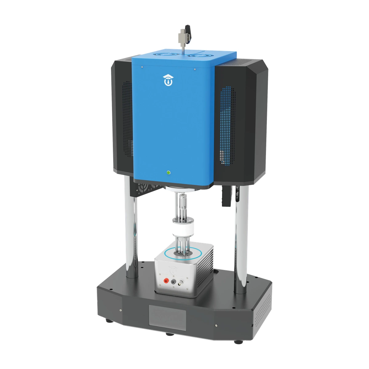
MatMeas RTS-1000C High-Temp Conductive Material Resistivity System (Upgraded from RMS-1000C)
The MatMeas RTS-1000C is the next-generation flagship evolution of the earlier RMS-1000C system, purpose-built for precision high-temperature conductive material resistivity measurement via four-wire Kelvin method. Delivering nΩ-to-MΩ resolution (10 nΩ to 100 MΩ) from RT to 600°C (±1°C PID), the upgraded platform features 99% zirconia thermal isolation, a rigid motorized test stand, and hybrid platinum/tungsten-carbide probes for vacuum and controlled atmospheres.
View details →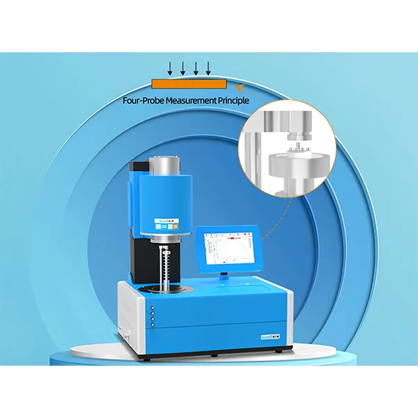
MatMeas RMS-1000P High-Temp Four-Point Probe Resistivity System
RMS-1000P uses four-point probe method for thin film and wafer resistivity measurement, featuring dual-electrostatic measurement, 0.1mΩ~100MΩ range, and specialized fixture for semiconductor materials.
View details →Request High-Precision Testing Solutions
Get expert guidance and customized instruments for your functional materials project.