High-Temperature Broadband Dielectric Testing of Ceramic Substrates
Technical News
Advanced ceramic substrates—predominantly high-purity alumina (Al2O3), aluminum nitride (AlN), silicon nitride (Si3N4), and low-temperature co-fired ceramics (LTCC)—form the structural, thermal, and dielectric foundation of modern high-power electronics and high-frequency microwave communications. From silicon carbide (SiC) traction inverters and 5G/6G millimeter-wave phased-array antennas to aerospace turbine engine telemetry and deep-well exploration sensors, these inorganic substrates must provide robust electrical isolation while simultaneously preserving signal integrity across harsh thermal environments.
Two primary electro-physical parameters dictate the performance of a ceramic substrate: relative dielectric permittivity (real permittivity, epsilon_r' or kappa) and dielectric loss tangent (dissipation factor, tan delta). The relative permittivity directly governs circuit capacitance, signal propagation delay (tau_pd roughly equals sqrt(epsilon_r') / c), and electromagnetic field containment in microstrip transmission lines. Concurrently, dielectric loss governs the proportion of high-frequency electromagnetic energy dissipated as waste heat, directly impacting insertion loss and thermal management in high-density power packages.
A widespread failure in electronic packaging design is assuming that dielectric permittivity and loss values quoted on supplier datasheets (typically measured at a single frequency, such as 1 MHz, at ambient room temperature 25 C) remain constant during operation. In real-world power modules, operating temperatures routinely exceed 150 C to 250 C, and can surge past 600 C in aerospace applications. Simultaneously, operating frequencies span from power-switching harmonics (10 kHz to 100 kHz) to RF communication bands (10 MHz to 30 MHz and beyond). Under these combined conditions, dielectric dispersion, thermally activated carrier conduction, and grain-boundary space charge relaxations cause dramatic shifts in electrical properties.
High-temperature broadband dielectric spectroscopy (BDS)—governed by ASTM D150, IEC 60250, and SEMI G44—is the definitive analytical methodology for mapping complex permittivity across wide frequency and temperature domains.
Complex Permittivity and Loss Deconvolution Equations
Under an applied alternating-current (AC) harmonic electric field E(t) = E_0 * exp(i * omega * t), the dielectric response of a ceramic substrate is mathematically described by the complex relative permittivity epsilon*(omega):
epsilon*(omega) = epsilon'(omega) - i * epsilon''(omega)
Where:
-
omega: The angular frequency of the applied AC field (omega = 2 * pi * f, in radians per second).
-
epsilon'(omega): The real permittivity (dielectric constant), which quantifies the reversible capacitive electrical energy storage capacity per unit volume:
epsilon'(omega) = C_p(omega) * d / (epsilon_0 * A)
Where C_p is the equivalent parallel capacitance, d is the substrate thickness, A is the active electrode area, and epsilon_0 is the vacuum permittivity (8.854 * 10^-12 F/m).
-
epsilon''(omega): The imaginary permittivity (dielectric loss factor), quantifying the irreversible electrical energy dissipated into heat per cycle.
The total dielectric loss tangent (tan delta) represents the ratio of dissipative to storage energy:
tan(delta) = epsilon''(omega) / epsilon'(omega)
Deconvolving Intrinsic Dipolar Loss from DC Conduction Loss
In polycrystalline ceramics at elevated temperatures, the measured imaginary permittivity epsilon''_total is not a pure reflection of microscopic dipole relaxation. Instead, it is composed of two physically distinct loss mechanisms:
epsilon''_total(omega) = epsilon''_dipole(omega) + sigma_dc / (epsilon_0 * omega)
Substituting this into the loss tangent expression yields:
tan(delta_total) = tan(delta_dipole) + sigma_dc / (omega * epsilon_0 * epsilon'(omega))
Where sigma_dc is the thermally activated direct-current electrical conductivity of the ceramic, and epsilon''_dipole encompasses atomic, electronic, and interfacial dipole relaxation processes.
This constitutive deconvolution reveals why dielectric loss surges exponentially at elevated temperatures and low frequencies (f < 1 kHz). Because electrical conductivity sigma_dc follows an Arrhenius thermal activation law (sigma_dc(T) = sigma_0 * exp(-E_a / (k_B * T))), mobile point defects (such as doubly ionized oxygen vacancies V_O_ddot in oxide ceramics or trace metallic impurities) gain high mobility above 200 C. At low frequencies, the 1 / omega term magnifies the conductive loss, causing apparent tan delta values to jump by several orders of magnitude. Broadband testing over multiple decades of frequency is essential to decouple genuine dielectric relaxation from background ohmic conduction.
Material Benchmark Comparison: Dielectric Properties Across Temperature
The following benchmark table illustrates the relative permittivity, dielectric loss, and thermal stability of standard ceramic substrate materials measured at 1 MHz at both room temperature and 500 C.
| Ceramic Substrate Material | Nominal Chemical Formulation | Relative Permittivity epsilon_r' (1 MHz, 25 C) | Relative Permittivity epsilon_r' (1 MHz, 500 C) | Loss Tangent tan delta (1 MHz, 25 C) | Loss Tangent tan delta (1 MHz, 500 C) | Thermal Expansion CTE (ppm/K) | Thermal Conductivity (W/m*K) | Primary Electronic Packaging Application |
|---|---|---|---|---|---|---|---|---|
| Alumina 96% (Al2O3) | 96% Al2O3 + silicate glassy phase | 9.2 to 9.5 | 10.4 to 10.8 | 0.0008 to 0.0012 | 0.0250 to 0.0450 | 7.1 | 24 to 28 | Automotive IGBT modules, industrial motor drives, thick-film power hybrids |
| High-Purity Alumina 99.6% | 99.6% alpha-Al2O3 (fine-grained) | 9.8 to 10.1 | 10.5 to 10.9 | 0.0001 to 0.0003 | 0.0035 to 0.0060 | 7.4 | 32 to 36 | Thin-film RF circuits, microwave monolithic integrated circuits (MMICs) |
| Aluminum Nitride (AlN) | >99% AlN + Y2O3 sintering aid | 8.8 to 9.1 | 9.6 to 10.0 | 0.0005 to 0.0008 | 0.0080 to 0.0150 | 4.6 | 170 to 220 | High-power traction inverters, laser diode submounts, SiC WBG power modules |
| Silicon Nitride (Si3N4) | beta-Si3N4 (gas-pressure sintered) | 7.8 to 8.2 | 8.5 to 8.9 | 0.0020 to 0.0035 | 0.0180 to 0.0300 | 3.2 | 80 to 90 | High-reliability EV traction inverters, military extreme thermal shock modules |
| Low-Temp Co-fired (LTCC) | Glass-bonded alumina composite | 5.8 to 7.5 | 6.8 to 8.6 | 0.0015 to 0.0030 | 0.0350 to 0.0650 | 5.8 | 2 to 5 | Multilayer RF radar modules, 5G transceiver front-ends, aerospace packaging |
| High-Purity Fused Silica | 99.99% amorphous SiO2 | 3.8 to 3.9 | 3.85 to 3.95 | < 0.0001 | 0.0004 to 0.0008 | 0.5 | 1.4 | High-frequency radomes, optical communication submounts, high-temp windows |
High-Temperature Fixture Architecture and OSL Calibration
Executing broadband impedance measurements up to 1000 C involves severe physical and electrical hurdles that do not exist at room temperature:
1. Residual Fixture Impedance and Lead Inductance
High-temperature test fixtures require long metallic extension leads (typically platinum, nickel-chromium, or pure silver) to span the distance from the hot furnace zone to the ambient-temperature instrument terminals. These physical extension leads introduce parasitic series resistance (R_lead) and series inductance (L_lead), while fixture electrode supports introduce stray parallel capacitance (C_stray) and conductance (G_stray).
At frequencies above 1 MHz, lead inductance resonates with sample capacitance, creating false resonant peaks that artificially elevate apparent permittivity. To eliminate these fixture artifacts, precision systems implement full Open-Short-Load (OSL) calibration:
Z_dut = (Z_meas - Z_short) / (1 - (Z_meas - Z_short) * Y_open)
Where Z_meas is the raw measured impedance vector, Z_short compensates for residual lead resistance and inductance, and Y_open compensates for fixture stray capacitance and leakage conductance. Performing OSL calibration at the actual test temperature ensures that the instrument reference plane is positioned directly at the sample faces.
2. Guarded Shielding and Electromagnetic Interference Suppression
Electric furnaces utilize powerful resistive heating elements (such as silicon carbide SiC rods or coiled resistance wire) that switch large AC currents. Without heavy electrostatic shielding, these high-current switching harmonics couple into the ultra-weak dielectric sensing leads, destroying the signal-to-noise ratio. Professional high-temperature spectrometers deploy grounded Faraday cages and coaxial shielding sleeves around all measurement leads.
Instrumentation Selection: DMS-1000 vs. DMS-2000 vs. CPS-7000
Matching testing requirements to the correct measurement platform ensures high data fidelity across diverse sample types. The matrix below compares the architectures of MatMeas' dedicated dielectric testing systems.
| System Specification | MatMeas DMS-1000 High-Temp Dielectric Spectrometer | MatMeas DMS-2000 Cryogenic-to-High-Temp Spectrometer | MatMeas CPS-7000 Dielectric Vacuum Micro-Probe Station |
|---|---|---|---|
| Temperature Envelope | Room Temperature to +1000 C (or +1200 C optional) | -160 C (liquid N2) up to +500 C (or +1000 C) | -160 C (liquid N2) up to +450 C (or +600 C) |
| Measurement Frequency Band | 20 Hz to 30 MHz (expandable to 120 MHz) | 10 uHz to 30 MHz | 20 Hz to 30 MHz (RF micro-probe tips) |
| Sample Geometry Compatibility | Bulk ceramic discs, square plates (diameter 10 mm to 30 mm) | Bulk discs, thick films, single crystals | Unpackaged micro-capacitors, patterned thin-film dice, wafer chips |
| Environmental Atmosphere | Air, flowing inert gas (Ar/N2), sealed vacuum | High-vacuum chamber (< 10^-3 Pa) or dry inert gas | High-vacuum chamber (< 10^-3 Pa) with optical view window |
| Cryogenic Frost Prevention | N/A (high-temperature dedicated) | High-vacuum insulation prevents moisture condensation | High-vacuum sealed stage completely eliminates frost artifacts |
| Contact Mechanism | Spring-loaded platinum parallel plate electrodes | Spring-loaded guarded platinum/gold electrodes | 4x micro-manipulated triaxial probe arms with pneumatic vibration isolation |
| Target Application | Sintered power substrates, refractory structural ceramics | Broad temperature screening, phase transition identification | In-situ microelectronic thin films, FeRAM cells, high-k dielectric gates |
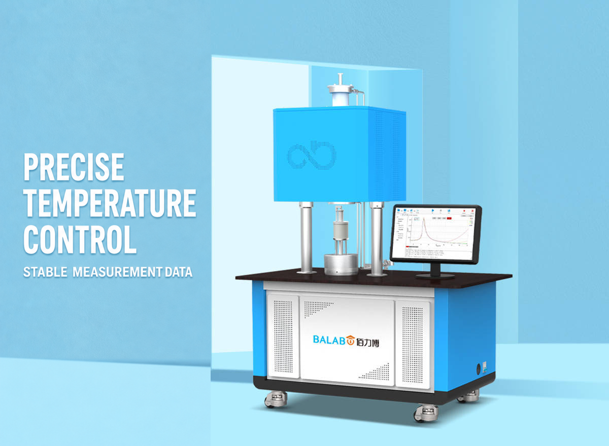
The flagship MatMeas DMS-1000 High-Temperature Dielectric Spectrometer serves as the primary characterization platform for power electronics substrates. Operating from 20 Hz to 30 MHz up to +1000 C, the DMS-1000 combines a heavy-gauge sealed metal shielding furnace with a coplanar thermocouple layout that positions the temperature sensor within 0.5 mm of the substrate face. This eliminates thermal lag errors during dynamic heating sweeps and delivers 0.05% basic impedance measurement accuracy.
For applications requiring characterization across deep cryogenic domains—essential for evaluating satellite electronics, cryogenic power grids, and superconducting power electronics—the MatMeas DMS-2000 High-Low Temperature Dielectric Spectrometer extends the measurement envelope from -160 C up to +500 C. The system incorporates a high-vacuum chamber that completely suppresses moisture condensation, preventing frost-induced parasitic surface capacitance from distorting cryogenic dielectric data.
When characterizing microscopic thin-film patterns, localized test keys on semiconductor wafers, or fragile MEMS elements, the MatMeas CPS-7000 High-Low Temperature Dielectric Vacuum Probe Station delivers high-precision micro-probing. Featuring four independently steered triaxial probe arms and integrated pneumatic anti-vibration damping, the CPS-7000 allows researchers to probe 20 um pads across a -160 C to +450 C thermal range without micro-probe drift or surface damage.
Standardized Step-by-Step SOP for Broadband Dielectric Testing
To achieve reproducible dielectric spectrum data conforming to ASTM D150 and IEC 60250, testing personnel must execute the following structured protocol:
Step 1: Specimen Preparation and Cleaning
- Fabricate ceramic substrate test specimens with strictly parallel faces (thickness variation < +/-0.005 mm across the entire surface). Recommended sample geometry is a circular disc with diameter 20.0 mm and thickness 0.5 mm to 1.0 mm.
- Polish opposing surfaces to a surface roughness Ra < 0.2 um to ensure intimate electrode contact without microscopic air gaps.
- Clean the specimen in an ultrasonic bath using acetone for 10 minutes, followed by 10 minutes in isopropanol. Bake at 150 C for 1 hour to drive off all adsorbed surface moisture, then cool inside a desiccator.
Step 2: Electrode Metallization
- Apply conductive thin-film electrodes to opposing faces to form a parallel-plate capacitor. Sputtered platinum or gold (100 nm thick with a 10 nm titanium adhesion layer) is recommended for temperatures up to 800 C.
- For measurements up to 1000 C, apply high-temperature platinum conductive paste and fire in a box furnace according to the manufacturer's thermal profile.
- Maintain a clean, unmetallized perimeter margin of at least 1.0 mm around the top electrode to eliminate edge flashover and lateral fringing leakage.
Step 3: Fixture Installation and OSL Compensation
- Prior to mounting the sample, execute Open and Short calibration across the full frequency spectrum (20 Hz to 30 MHz) using the high-temperature fixture leads inside the test chamber.
- Mount the metallized ceramic substrate centrally between the parallel platinum contact plates. Apply moderate mechanical spring pressure (typically 1 N to 2 N) to ensure intimate contact without mechanical fracture.
- Verify that the ambient room-temperature capacitance C_p and loss tangent tan delta align with anticipated theoretical values.
Step 4: Temperature Programming and Broadband Acquisition
- Program the temperature controller with defined thermal setpoints (e.g., from 25 C to 800 C in 50 C increments, at a controlled heating ramp of 2 C/min to 5 C/min).
- At each thermal setpoint, enforce an isothermal dwell period of at least 5 minutes to guarantee complete thermal equilibrium throughout the ceramic specimen thickness.
- Execute automated logarithmic frequency sweeps (e.g., 50 frequency points per decade from 20 Hz to 30 MHz).
- Continuously log parallel capacitance C_p, dissipation factor tan delta, equivalent series resistance (ESR), real permittivity epsilon', and imaginary permittivity epsilon''.
Frequently Asked Questions (FAQ)
Why does the dielectric loss of a ceramic substrate increase dramatically at high temperatures?
At room temperature, electrical loss is dominated by intrinsic dipolar polarization. As temperature rises above 200 C to 400 C, intrinsic point defects (such as oxygen vacancies V_O_ddot) and trace ionic impurities gain sufficient thermal energy to jump across crystalline barriers. This activates DC electrical conductivity (sigma_dc), which contributes an electrical loss term proportional to sigma_dc / (omega * epsilon_0). At low frequencies, this conductive loss term causes apparent tan delta to jump by orders of magnitude.
How does fixture lead inductance distort high-frequency permittivity measurements?
At frequencies above 1 MHz, the physical inductance of high-temperature metallic extension leads (L_lead) combines with the capacitance of the ceramic specimen (C_dut) to form a series resonant circuit. As the test frequency approaches the self-resonant frequency f_0 = 1 / (2 * pi * sqrt(L_lead * C_dut)), the measured capacitance appears to increase dramatically, creating false permittivity peaks. Implementing Open-Short-Load (OSL) calibration at the sample terminals cancels out L_lead and restores true flat permittivity spectra.
What is the advantage of using sputtered platinum electrodes over silver paste for testing up to 800 C?
Conductive silver paste begins to soften and oxidize above 400 C to 500 C, and silver ions rapidly migrate into ceramic grain boundaries under an applied electric field, creating false leakage paths. Sputtered thin-film platinum possesses a melting point of 1768 C, does not oxidize in air at 800 C, and exhibits negligible solid-state diffusion into alumina or nitride lattices, ensuring a stable, non-reactive electrical contact interface.
Why is an isothermal dwell time mandatory at each temperature setpoint during frequency sweeps?
Technical ceramics have finite thermal conductivity and heat capacity, while furnace thermocouple probes are positioned in the adjacent gas space or fixture metal. During continuous ramping, thermal lag causes the internal core of the ceramic to lag behind the measured thermocouple reading. Enforcing an isothermal dwell of 3 to 5 minutes guarantees that the entire specimen reaches uniform thermal equilibrium before the frequency sweep executes.
Related Instruments & Equipment
MatMeas DMS1000 High-Temperature Dielectric Spectrometer
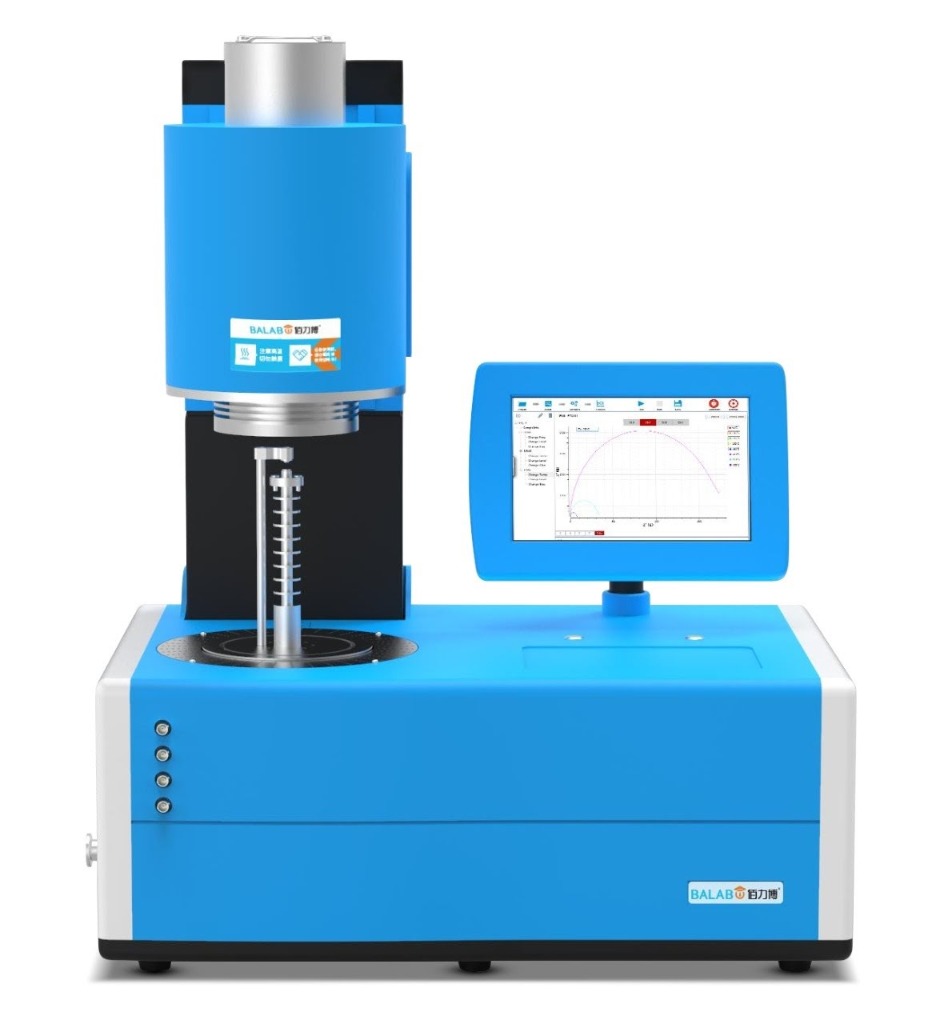
The MatMeas DMS1000 is an advanced High-Temperature Dielectric Impedance Temperature Spectrometer engineered for the ultimate electrical characterization of bulk materials. Delivering an exceptional measurement accuracy of 0.05%, it operates efficiently from Room Temperature (RT) to 1000°C. Its upgraded platform supports both single-sample and four-sample simultaneous measurements. Integrated with a sealable metal shielding system and high-purity platinum electrodes, the DMS1000 enables highly reliable testing across inert, oxidizing, reducing, and vacuum atmospheres, making it an indispensable infrastructure for precision materials science.
View details →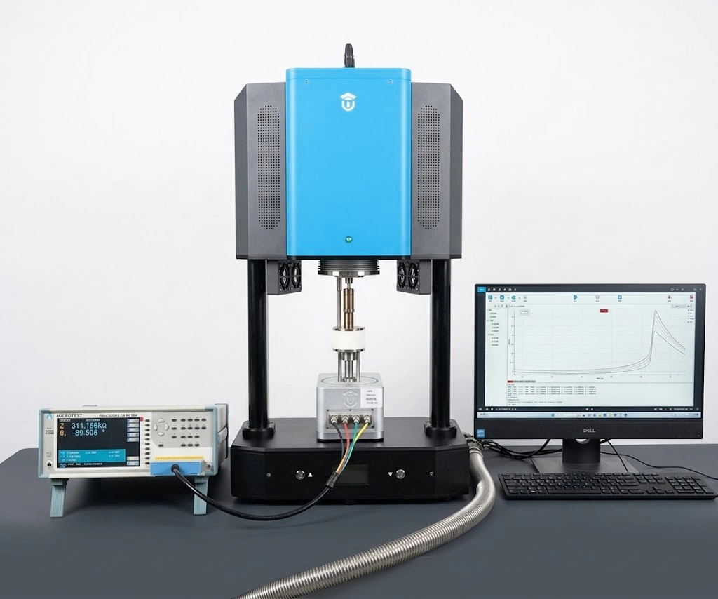
MatMeas DTS1000 High-Temperature Dielectric Impedance Spectrometer
Built on the proven DMS series platform, the MatMeas DTS1000 is a next-generation high-temperature dielectric impedance spectrometer engineered specifically for high-temperature mechanistic research on functional ceramics and advanced dielectric materials. Its modular architecture supports effortless plug-and-play switching between single-channel precision measurement and four-channel high-throughput screening. Across a wide temperature range from room temperature to 1000°C, the DTS1000 delivers fully automated, high-accuracy mapping of dielectric constant, dielectric loss, Curie temperature, and Cole-Cole/Nyquist spectra.
View details →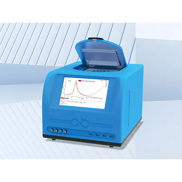
MatMeas DMS2000 High-Low Temperature Dielectric Spectrometer
The MatMeas DMS2000 is an advanced High and Low Temperature Dielectric Impedance Spectrometer engineered for evaluating the dielectric properties of materials under extreme thermal conditions. Compliant with the ASTM D150 standard, it integrates a proprietary LNP-95 liquid nitrogen injection system to achieve seamless continuous temperature variation from -160°C to 450°C. Uniquely featuring a vacuum-enabled sample chamber to completely prevent thermal frosting and eliminate false water peaks near 0°C, along with versatile options for single-sample or five-sample simultaneous testing, the DMS2000 ensures unparalleled data fidelity and high throughput for advanced scientific research.
View details →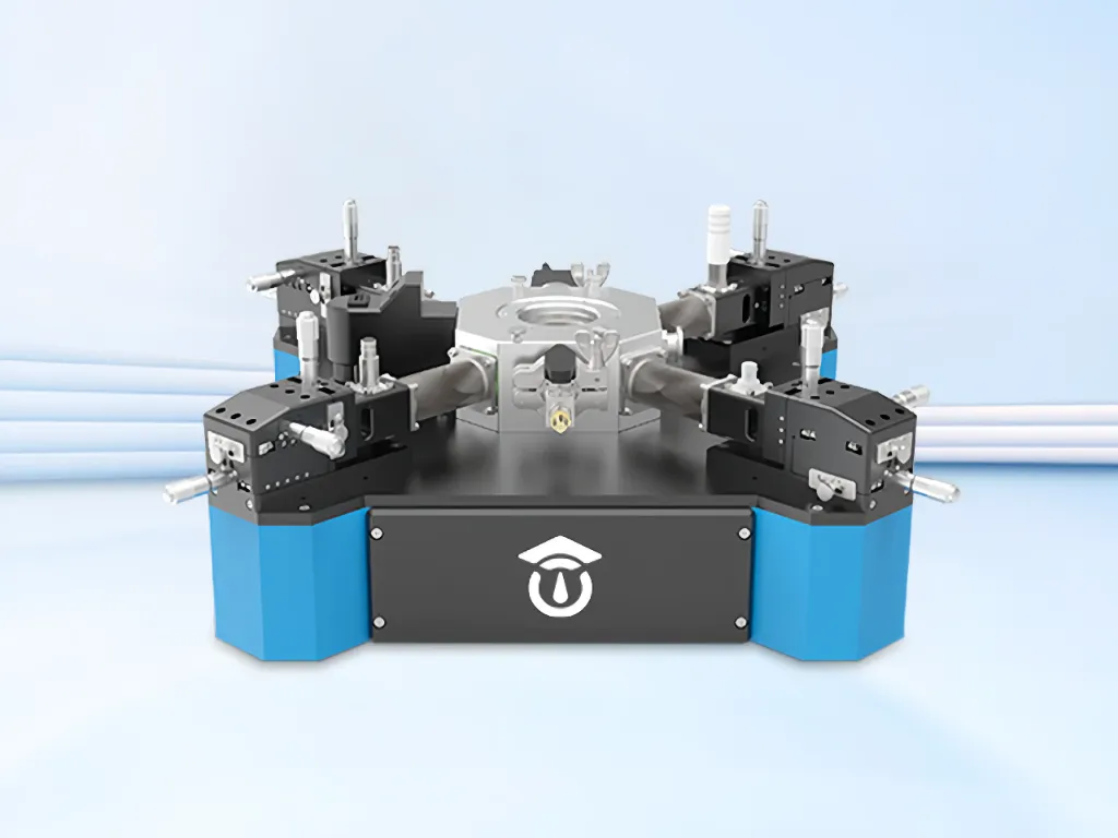
CPS7000 High-Low Temperature Dielectric Vacuum Probe Station
The MatMeas CPS7000 is an advanced, highly integrated desktop High-Low Temperature Dielectric Vacuum Probe Station engineered for the rigorous electrical characterization of thin films, bulk materials, and semiconductor wafers. Delivering performance directly comparable to industry-leading American brands like Lake Shore and Janis, this compact platform offers an ultra-wide temperature range from -160°C to 450°C via liquid nitrogen cooling. Uniquely equipped with a proprietary built-in air shock anti-vibration system, the CPS7000 eliminates data jumping points during continuous temperature variations. Supporting complex high-voltage and low-current testing environments, it is the ultimate infrastructure for evaluating dielectric, piezoelectric, ferroelectric, and TSDC properties in high-vacuum conditions.
View details →Request High-Precision Testing Solutions
Get expert guidance and customized instruments for your functional materials project.