How to Pole Novel 1–5 μm Piezoelectric Thin Films on FTO/ITO and Flexible Substrates: Engineering Selection Guide
Technical News
Advanced functional electronics, wearable biomechanical harvesters, and acoustic microsystems increasingly demand environmentally sustainable materials. Consequently, research teams across global universities are aggressively exploring novel lead-free organic–inorganic piezoelectric thin films. Deposited on conductive fluorine-doped tin oxide (FTO) or indium tin oxide (ITO) glass substrates, or on flexible polymeric supports, these emerging material systems represent the frontier of micro-electromechanical systems (MEMS).
However, translating newly synthesized lead-free thin films into functional piezoelectric elements introduces acute manufacturing bottlenecks. Unlike bulk ceramics that withstand straightforward mechanical clamping and immersion in high-temperature dielectric oil baths, thin films ranging from 1 μm to 5 μm in thickness present severe dielectric vulnerability. Standard poling methodologies frequently trigger dielectric puncture, edge flashover, and mechanical fracture under high electric fields.
This technical engineering guide explores the physics, equipment trade-offs, and experimental protocols required to successfully pole 1–5 μm piezoelectric films. Synthesizing practical engineering consultations for academic research teams developing advanced functional thin films, this guide evaluates non-contact corona discharge against in-plane contact probe poling, resolves common literature discrepancies, and establishes an experimental standard operating procedure (SOP) for materials with unestablished poling parameters.
The Engineering Challenge: Microscopic Films on Conductive and Flexible Substrates
When a laboratory synthesizes an organic–inorganic hybrid piezoelectric material, the primary goal is aligning randomly oriented crystalline dipoles to establish remanent macroscopic polarization. The physical challenge intensifies dramatically when operating within the 1–5 μm thickness regime on conductive substrates:
-
Catastrophic Pinhole Vulnerability: Sub-5 μm solution-cast or vapor-deposited thin films inevitably exhibit microscopic pinholes, localized grain boundaries, or thickness non-uniformities. In a conventional contact poling arrangement with sputtered top and bottom metallic electrodes, applying a high voltage across a pinhole initiates an immediate electrical arc. This localized arc discharges the energy stored across the entire capacitor, causing thermal runaway that vaporizes the metallization and destroys the specimen.
-
Substrate Clamping and Mechanical Strain: When deposited on rigid 1" × 1" FTO/ITO-coated glass substrates, piezoelectric films experience mechanical clamping from the substrate. In accordance with the Lefki-Dormans substrate clamping relation, the effective longitudinal piezoelectric coefficient
d33_fmeasured on a clamped substrate is suppressed relative to intrinsic bulk coefficients:
d33_f = d33 - [2 * ν / (1 - ν)] * d31
Here, ν represents the Poisson ratio of the film, and d31 is the transverse piezoelectric coefficient. Poling fields must overcome this substrate-induced mechanical stress to successfully orient internal ferroelectric domains.
-
Absence of Top Electrodes during Early Iterations: In early-stage chemical formulation research, fabricating patterned, photolithographic top electrodes is time-consuming and expensive. Researchers require an agile polarization methodology that polarizes the bare film surface directly without requiring top metallization.
-
Thermal Constraints of Flexible Substrates: When transitioning from rigid FTO glass to flexible polymeric substrates (such as polyimide, PEN, or PET), processing temperatures must strictly adhere to the thermal degradation and glass transition limits of the organic backing (typically below 150°C).
Application Requirements Matrix
To define the hardware design envelope, initial research specifications must be categorized into mechanical, electrical, and thermal boundary conditions. The table below outlines the core requirements established during typical thin-film poling evaluations:
| Parameter Specification | Current Baseline Requirement | Future Planned Scope | Critical Engineering Constraint |
|---|---|---|---|
| Material Chemistry | Lead-free organic–inorganic hybrid | Multiferroic composites | High chemical sensitivity; moisture and ozone exposure limits |
| Film Thickness Range | 1.0 μm to 5.0 μm | Sub-micron (< 1.0 μm) | Extreme dielectric breakdown sensitivity; pinhole arcing |
| Substrate Architecture | 1" × 1" × 1 mm FTO/ITO glass | Flexible polymeric foil | Requires continuous bottom grounding; anti-curl fixturing |
| Maximum Active Area | 25.4 mm × 25.4 mm (1" × 1") | Multi-coupon scanning | Uniform surface charge deposition without edge field peaks |
| Electrode Configuration | Un-metallized top surface | Interdigitated electrodes (IDE) | Through-thickness corona field vs. in-plane contact field |
| Target Electric Field | Not yet established | Variable (5 to 100 MV/m) | Requires broad, finely adjustable voltage headroom |
| Thermal Operating Window | Ambient up to 150°C | Cryogenic to 200°C | PID regulation accuracy within ±0.5°C to ±3°C |
| Voltage Holding Time | 5 to 60 minutes | Automated multi-dwell | Controlled field-cooling under sustained polarization |
Resolving the Literature Gap: Why Published Electric Fields Differ from Equipment Voltages
A frequent point of confusion among research chemists and materials scientists involves converting values reported in academic literature into operational equipment setpoints. When evaluating novel functional materials, research papers typically cite values such as:
- Coercive electric fields measured on single crystals (e.g.,
Ec ≈ ±4 kV/mmor40 kV/cm); - Localized polarization switching voltages recorded via Piezoresponse Force Microscopy (PFM) (e.g.,
V_switch ≈ ±3 Vto±5 V).
While these metrics provide valuable fundamental references, treating them as direct equipment specifications for macroscopic thin-film poling is an engineering mistake.
The Microscopic PFM vs. Macroscopic Film Dilemma
PFM measurements utilize an atomically sharp conductive cantilever tip with an apex radius of curvature of 10 nm to 50 nm. When a 3 V bias is applied across a 50 nm radius tip in direct contact with a film, the electric field directly beneath the tip apex is localized and inhomogeneous, easily exceeding 100 MV/m (1 MV/cm).
Conversely, a macroscopic thin-film poling system must polarize a continuous 25 mm × 25 mm area uniformly. In macroscopic samples:
- Dielectric Thickness Scaling: The uniform macroscopic electric field
Eestablished across a thin film of thicknessdis governed by:
E = V_film / d
For a 2 μm (2 × 10⁻⁶ m) thin film, generating an electric field of 50 MV/m (equivalent to 50 kV/mm) requires an effective potential difference across the film of:
V_film = 50 × 10⁶ V/m × 2 × 10⁻⁶ m = 100 V
If the material coercive field were truly 4 kV/mm (4 MV/m), the required theoretical film voltage would be merely 8 V.
- Interfacial Depolarization and Surface Potential: In non-contact corona poling, the voltage supplied by the high-voltage generator (
0 to −30 kV) does not fall directly across the 2 μm film. Instead, the voltage drops predominantly across the ambient air gap between the ionization emitter and the film surface. The air ionizes according to Paschen's Law, creating a charge flux that deposits surface ions (typicallyCO3⁻orO2⁻species in negative corona). The actual electric field driving domain orientation depends on surface charge densityσand relative dielectric permittivityεr:
E_internal = σ / (ε0 * εr)
Therefore, a high-voltage corona power supply capable of −30 kV is necessary to generate stable gas ionization and drive ion flux through the control grid, even though the electrostatic potential clamped on the film upper surface may only range from 50 V to several hundred volts.
- Defect-Mediated Breakdown Limits: In bulk single crystals, crystalline perfection permits high intrinsic dielectric strength. In polycrystalline or organic–inorganic thin films, dielectric strength complies with the empirical scaling relation governed by ASTM D149 and IEC 60243:
E_breakdown ∝ d^(-0.5)
Although thinner films theoretically sustain higher electric field densities than thick bulk ceramics, real-world defects require dynamic, closed-loop current limitation to prevent localized flashovers from propagating into macroscopic failures.
Architectural Trade-Off: Non-Contact Corona Poling vs. In-Plane Probe Station Poling
Depending on whether the thin film is fabricated with or without a conductive top electrode, and whether the intended domain orientation is through-thickness or in-plane, laboratories must select between two primary instrumentation architectures.
                    ┌───────────────────────────────────────────────┐
                    │  1–5 μm Thin Film Poling Architectural Choice │
                    └───────────────────────┬───────────────────────┘
                                            │
                             Top Electrode State on Sample?
                                            │
                     ┌──────────────────────┴──────────────────────┐
                     ▼                                             ▼
             [No Top Electrode]                           [Top Electrode Deposited]
                     │                                             │
      Substrate: FTO / ITO Glass                      Geometry: Through-Thickness or IDE?
                     │                                             │
                     ▼                              ┌──────────────┴──────────────┐
      [Through-Thickness Poling]                    ▼                             ▼
       MatMeas FCP Corona System           [Planar Capacitor]           [In-Plane Comb / IDE]
   • Non-contact virtual electrode       • High-voltage contact        • Micro-probe contact
   • Negative Trichel self-quenching     • Guarded probe tips          • Inter-digit spacing control
   • Zero pinhole spark-over             • Liquid N2 / Heated stage    • High-vacuum spark suppression
   • Up to -30 kV / 150°C chuck          • −160°C to 450°C             • MatMeas CPS7000 Station
Solution 1: Non-Contact Corona Poling (MatMeas FCP Platform)
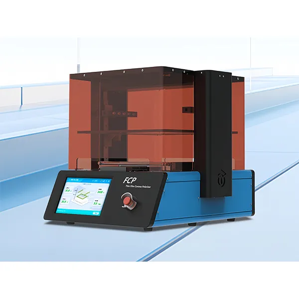
For thin films deposited directly on conductive FTO or ITO glass substrates without a top metallic electrode, the MatMeas FCP Thin Film Corona Polarizer provides the primary non-destructive solution.
In this architecture, the conductive FTO/ITO coating serves as the grounded counter-electrode. The specimen rests directly upon the temperature-controlled ground stage. The FCP system applies a high negative DC potential (0 to −30 kV / 2 mA) to a proprietary non-contact discharge emitter suspended above the sample.
Key physical advantages include:
-
Trichel Pulse Self-Limiting Stability: Negative corona discharge operates via high-frequency, self-quenching Trichel pulses. If a microscopic pinhole exists in the 1–5 μm film, the localized electrostatic charge simply discharges harmlessly through the pinhole to the conductive FTO base. Unlike contact poling, there is no conductive metallic top layer to feed large currents into the defect. The discharge remains strictly microscopic and self-healing.
-
Dual-Power Grid Potential Clamping: The FCP incorporates two built-in, electrically isolated power supplies. The primary module energizes the corona ionization wire, while an independent auxiliary module biases a metallic governing grid positioned above the specimen. The grid clamps the maximum surface potential deposited on the film, ensuring that the electric field across the 1" × 1" coupon remains uniform within ±5%.
-
Thermal Domain Activation: Incorporating the optional FCPHT150 stage provides closed-loop PID heating up to 150°C with selectable ramps (3°C/min, 6°C/min, 9°C/min). This allows researchers to elevate temperatures toward the material dipole relaxation point, apply the polarizing field, and maintain the field while cooling back to room temperature.
Solution 2: In-Plane and Contact Probe Poling (MatMeas CPS7000 Platform)
When experimental protocols require in-plane domain alignment via interdigitated electrodes (IDE), or when micro-scale top capacitor pads have been photolithographically deposited, non-contact corona discharge is unsuitable. In-plane polarization requires the MatMeas CPS7000 High-Low Temperature Vacuum Probe Station coupled with an external high-voltage DC source.
In an interdigitated electrode geometry, alternating metallic fingers are deposited onto the film surface with micro-scale spacing (w_gap = 5 μm to 50 μm). When a high voltage V_bias is applied across adjacent fingers:
E_inplane ≈ V_bias / w_gap
With an electrode gap of 10 μm, applying merely 500 V establishes an intense in-plane field of 50 MV/m.
Key physical advantages of the CPS7000 platform include:
-
High-Vacuum Arc Suppression: Applying high voltages across narrow 5–10 μm gaps in ambient air risks immediate air breakdown (spark-over). By operating inside a sealed high-vacuum chamber (< 10⁻² Pa), the mean free path of gas molecules exceeds electrode spacing, suppressing Paschen electrical breakdown and permitting high lateral fields.
-
Vibration-Isolated Probing: Landing micro-manipulated tungsten or beryllium-copper probe tips onto delicate 1–5 μm thin films on glass requires precise contact force. The CPS7000 features a proprietary internal pneumatic air-shock anti-vibration system that isolates probe arms from ambient floor vibrations. This eliminates probe jumping, micro-scratching, and electrode delamination during thermal cycling.
-
Broad Thermal Operating Envelope: Supporting liquid nitrogen cooling and resistive heating from −160°C to 450°C with ±0.5°C stability, the CPS7000 allows researchers to evaluate dielectric phase transitions, Curie points, and Thermally Stimulated Depolarization Current (TSDC) across extreme temperature spectra.
Hardware Selection Matrix: FCP vs. CPS7000
The table below contrasts the mechanical, electrical, and operational capabilities of the two poling systems:
| Architectural Feature | MatMeas FCP Thin Film Polarizer | MatMeas CPS7000 Vacuum Probe Station |
|---|---|---|
| Primary Poling Principle | Non-contact negative corona discharge | Direct micro-contact electrical probing |
| Polarization Direction | Through-thickness (transverse) | In-plane (IDE) or through-thickness capacitor |
| Electrode Requirement | Bottom conductive substrate only (FTO/ITO) | Micro-patterned top electrodes or IDE pads |
| Maximum Applied Voltage | 0 to −30 kV DC (continuous) | Up to ±5 kV DC (with external HV source) |
| Sample Size / Active Area | 200 mm × 200 mm (coupons up to 1" × 1") | Samples up to φ 40 mm, thickness < 5 mm |
| Temperature Range | Ambient to 150°C (FCPHT150 stage) | −160°C to 450°C (Liquid N2 + resistive heater) |
| Temperature Stability | ±3.0°C | ±0.5°C |
| Environmental Control | Amber interlocked air chamber | High vacuum (< 10⁻² Pa) or inert atmosphere |
| Optical Alignment | Top overview observation | In-situ φ 55 mm high-purity quartz window |
| Vibration Isolation | Heavy rigid baseplate | Proprietary integrated air-shock mechanism |
| Thin-Film Breakdown Risk | Low (self-limiting charge dissipation) | Moderate to High (requires vacuum arc suppression) |
| Primary Research Fit | Un-metallized films on FTO/ITO & flexible foil | Interdigitated in-plane poling & micro-capacitors |
Standard Operating Procedure: Poling Materials with Unknown Conditions
For newly synthesized functional materials where coercive field, Curie temperature, and breakdown thresholds have not been established in literature, researchers should execute a standardized step-wise optimization protocol:
[Phase 1: Room-Temp Leakage Profiling]
Apply low DC voltage (10–50 V). Monitor I-V curve to establish baseline leakage current.
                  │
                  ▼
[Phase 2: Step-Wise Electric Field Sweeps]
Increase field in 5 MV/m increments at room temperature. Detect onset of non-linear conduction.
                  │
                  ▼
[Phase 3: Thermal Dipole Activation Ramps]
Elevate sample stage in 20°C steps. Hold 15 min at each dwell to permit chain relaxation.
                  │
                  ▼
[Phase 4: Field-Sustained Cooling Protocol]
Maintain target poling field. Cool sample below 40°C under full field to freeze dipole alignment.
                  │
                  ▼
[Phase 5: Metrology & Piezoelectric Verification]
Evaluate quasi-static d33 coefficient or PFM phase retention after 24h room-temperature aging.
Phase 1: Pre-Poling Leakage and Capacitance Baseline
Before exposing delicate 1–5 μm thin films to intense electric fields, measure the room-temperature low-field capacitance Cp and loss tangent tanδ (using an LCR meter at 1 kHz). Highly lossy films (tanδ > 0.05) contain excessive mobile ions, free carriers, or solvent residues. Poling a lossy film results in Joule heating and thermal breakdown rather than dipole alignment. If loss is elevated, anneal the substrate under vacuum to drive out moisture.
Phase 2: Electric Field Threshold Sweep
Begin corona or contact poling at a conservative field:
- Set the initial surface potential to produce
E ≈ 10 MV/m(e.g., 20 V across a 2 μm film). - Dwell for 5 minutes while monitoring leakage current or corona discharge stability.
- Increment the electric field in steps of
5 MV/muntil reaching50% to 70%of the expected dielectric breakdown strength. In negative corona poling, adjust the grid bias to elevate the clamped surface potential incrementally.
Phase 3: Isofield Thermal Soaking
Once the film demonstrates stable insulation resistance under moderate fields, activate thermal heating:
- Ramp temperature at
3°C/minunder closed-loop PID control toward the estimated relaxation temperature (typically 60°C to 110°C for organic–inorganic hybrids). - Maintain the sample at the dwell temperature for 15 to 30 minutes. Thermal agitation lowers domain switching energy barriers, enabling cooperative dipole reorientation along the applied field vector.
Phase 4: Field-Cooling Lock-In
Critical Experimental Rule: Never remove the electric field while the specimen remains elevated in temperature. Thermal energy at elevated temperatures will rapidly randomize aligned dipoles, nullifying remanent polarization.
- Maintain the full high-voltage corona or contact potential across the film.
- Initiate controlled cooling of the ground stage back to ambient room temperature (below 35°C–40°C).
- Only after the stage has stabilized at room temperature should the high-voltage supply be de-energized.
Phase 5: Aging and Piezoelectric Verification
Allow the polarized film to rest for 24 hours at room temperature with grounded electrodes to dissipate residual surface space charges. Subsequently, measure the remanent longitudinal piezoelectric coefficient d33 via a quasi-static Berlincourt meter or evaluate localized domain stability via PFM.
Troubleshooting Laboratory Failure Modes
The table below outlines common failure modes encountered during thin-film poling, their physical root causes, and corrective instrumentation actions:
| Failure Symptom | Physical Root Cause | Corrective Engineering Action |
|---|---|---|
| Instantaneous Pinhole Arc | Sputtered top metal feeds avalanche current through local thickness void | Switch to non-contact negative corona poling (FCP); eliminate top metallization |
| Edge Spark-Over / Flashover | Severe field fringing along 1" × 1" glass perimeter exceeding air breakdown | Install customized insulating perimeter shield; ensure FTO edge margin is ≥ 2 mm |
| Substrate Curling / Warping | Thermal expansion mismatch between thin film and flexible polymer substrate | Reduce heating ramp to 3°C/min; engage low-stress edge clamping fixture on FCP stage |
| Zero Remanent Piezoelectricity | Voltage de-energized before sample cooled; thermal dipole relaxation | Enforce strict field-cooling protocol: maintain voltage until chuck cools below 35°C |
| Excessive Surface Leakage | Ambient moisture adsorption or airborne dust on un-electroded film surface | Execute pre-poling dry nitrogen purge or brief vacuum bakeout at 80°C |
| Probe Micro-Scratch on Film | Mechanical building vibrations coupled through probe arm during thermal sweep | Engage CPS7000 integrated pneumatic air-shock isolation; adjust probe spring compliance |
Dual-Funnel Conversion: Instrument Acquisition vs. Testing Services
Equipping a research laboratory for advanced thin-film polarization requires matching instrumentation capabilities to project timelines and available funding:
1. Turnkey Capital Equipment Acquisition
For universities, research institutes, and industrial R&D centers establishing permanent materials characterization infrastructure, MatMeas provides fully validated hardware platforms:
- For Through-Thickness Thin-Film Poling: The MatMeas FCP Thin Film Corona Polarizer is the dedicated platform for 1–5 μm films on FTO/ITO glass and flexible foils. Configured with the FCPHT150 heating stage and customized 1" × 1" substrate holders, it delivers complete, arc-free dipole orientation.
- For In-Plane Interdigitated Poling: The MatMeas CPS7000 High-Low Temperature Vacuum Probe Station provides the requisite high-vacuum environment, vibration-isolated micro-probing, and wide thermal range (−160°C to 450°C) to prevent electrical breakdown across narrow electrode spacings.
To request a formal quotation, technical engineering consultation, or customized substrate fixture drawings, submit an equipment inquiry via the product pages.
2. Preliminary Validation via MatMeas Testing Services
For academic research groups currently formulating initial chemical recipes, working with unestablished poling parameters, or awaiting dedicated capital equipment grant funding, MatMeas provides a low-barrier alternative:
Submit your raw film coupons to MatMeas Laboratory Testing Services. Our factory applications laboratory will conduct pilot corona poling sweeps, establish optimal field-temperature-time profiles, and provide calibrated post-poling piezoelectric and ferroelectric characterization reports before you commit capital expenditure.
Frequently Asked Questions
Can thin films only 1–5 μm thick deposited on conductive FTO/ITO glass be poled without top electrodes?
Yes. Non-contact negative corona poling using the MatMeas FCP platform is specifically engineered for this configuration. The conductive FTO or ITO coating on the glass substrate serves as the grounded base electrode, while ionized atmospheric charges deposited across the bare film surface act as a virtual top electrode. This eliminates the expense of top metallization and fundamentally prevents catastrophic pinhole punch-through.
Why do published single-crystal coercive fields differ from macroscopic thin-film poling voltages?
Single crystals exhibit high crystalline purity and lack substrate clamping, yielding intrinsic coercive fields. In macroscopic thin films, grain boundaries, interface depolarization fields, and mechanical substrate clamping suppress domain rotation. Furthermore, microscopic PFM voltage values (e.g., ±3 V) apply across nanometer-scale tip radii, creating localized field densities exceeding 100 MV/m that cannot be directly correlated to macroscopic voltage setpoints without accounting for film thickness, electrode architecture, and air-gap ionization drops.
How should a research team optimize poling temperature and holding time when conditions are unknown?
Researchers should implement an iterative, step-wise protocol: evaluate room-temperature leakage current first, increment the applied field in 5 MV/m steps, and then elevate temperature in 20°C stages up to the polymer glass transition or ceramic relaxation threshold. Crucially, researchers must follow a field-sustained cooling schedule, maintaining the high-voltage field continuously until the substrate stage cools below 35°C–40°C to lock in aligned dipoles.
When should a laboratory select the FCP corona poler versus the CPS7000 vacuum probe station?
The decision depends on electrode architecture and field direction. If the thin film is deposited on a conductive substrate (FTO/ITO or metal foil) without top electrodes and requires through-thickness polarization, the MatMeas FCP corona system is the primary choice. If the thin film features photolithographically patterned interdigitated electrodes (IDE) for in-plane polarization, or requires micro-probing under high vacuum to suppress air arcing across micro-scale gaps, the MatMeas CPS7000 vacuum probe station is the required platform.
Related Instruments & Equipment
MatMeas FCP Thin Film Corona Polarizer
The MatMeas FCP Thin Film Corona Polarizer is an advanced laboratory platform specifically engineered for high-efficiency polarization of piezoelectric polymer films (e.g., PVDF, P(VDF-TrFE)). Delivering 0 to −30 kV / 2 mA negative corona discharge across a spacious 200 mm × 200 mm active poling area, it features dual independent power modules to eliminate electrical cross-talk and utilizes an innovative non-contact single-wire electrode fixture. With optional FCPHT150 high-temperature heating stage (≤ 150°C, precision ≤ ±3°C) and FCPOP01 smart suite supporting remote OTA updates and API integration, the FCP uniformly polarizes ultra-thin films (5 μm to 200 μm, ideally 10–50 μm) from custom coupons (e.g., 50 mm × 50 mm) up to 200 mm × 200 mm sheets without dielectric breakdown.
View details →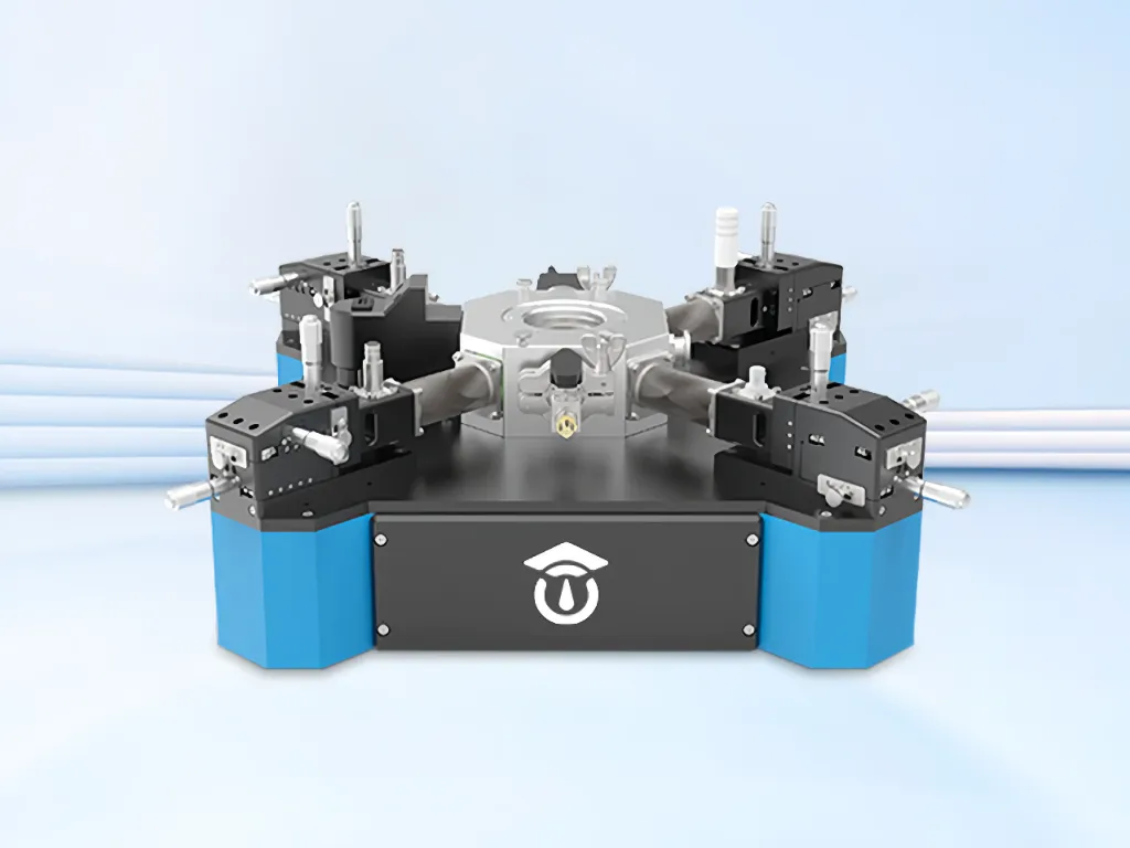
CPS7000 High-Low Temperature Dielectric Vacuum Probe Station
The MatMeas CPS7000 is an advanced, highly integrated desktop High-Low Temperature Dielectric Vacuum Probe Station engineered for the rigorous electrical characterization of thin films, bulk materials, and semiconductor wafers. Delivering performance directly comparable to industry-leading American brands like Lake Shore and Janis, this compact platform offers an ultra-wide temperature range from -160°C to 450°C via liquid nitrogen cooling. Uniquely equipped with a proprietary built-in air shock anti-vibration system, the CPS7000 eliminates data jumping points during continuous temperature variations. Supporting complex high-voltage and low-current testing environments, it is the ultimate infrastructure for evaluating dielectric, piezoelectric, ferroelectric, and TSDC properties in high-vacuum conditions.
View details →Request High-Precision Testing Solutions
Get expert guidance and customized instruments for your functional materials project.