Ceramic Substrate Resistivity Testing: Cryogenic to High Temperature
Technical News
Advanced technical ceramic substrates—primarily polycrystalline alumina (Al2O3), aluminum nitride (AlN), silicon nitride (Si3N4), and beryllium oxide (BeO)—form the critical structural, thermal, and dielectric isolation backbone of modern power electronics. In high-power traction inverters for electric vehicles, silicon carbide (SiC) and gallium nitride (GaN) third-generation semiconductor packaging, aerospace avionics, and deep-well energy exploration, these substrates are subjected to extreme operating thermal spans. Temperatures can plunge to sub-zero and cryogenic baselines (-40°C to -160°C) during unpowered high-altitude flight or deep-space transit, then escalate rapidly to 300°C, 600°C, or well above 1000°C under heavy continuous power switching.
At room temperature, high-purity ceramic substrates act as exceptional insulators, routinely exhibiting volume resistivities in excess of 10^14 Ω·cm. However, electrical resistivity is not static; it is an exponentially varying thermodynamic function of temperature. While cryogenic exposure introduces thermal contraction mismatches, brittle interfacial micro-cracking, and frost-induced surface tracking, extreme temperatures activate internal defect hopping, collapsing bulk volume resistivity by up to ten orders of magnitude. Evaluating electrical insulation across this entire thermal spectrum—in strict compliance with ASTM D257, ASTM D1829, and IEC 60093 standards—is mandatory to establish safe operating boundaries and prevent catastrophic thermal-electric runaway.
Physical Mechanisms Governing Electrical Conduction Across Temperature
Electrical transport in inorganic polycrystalline ceramics transitions through distinct physical conduction regimes across the thermal spectrum, described mathematically by dual-activation Arrhenius kinetics:
σ(T) = σ_ext * exp[ -E_ext / ( k_B * T ) ] + σ_int * exp[ -E_int / ( k_B * T ) ]
where σ(T) is total electrical conductivity (the reciprocal of volume resistivity, σ = 1 / ρ_v), σ_ext and σ_int are pre-exponential factors, E_ext and E_int are characteristic thermal activation energies, k_B is the Boltzmann constant (8.617 * 10^-5 eV/K), and T is absolute temperature in Kelvin.
- Low-Temperature & Cryogenic Regime (-160°C to 0°C): Charge carriers (electrons, holes, and impurity ions) are thermodynamically frozen in localized defect traps. Conduction is dominated by quantum-mechanical Mott variable-range hopping between localized states. In this regime, intrinsic bulk resistivity exceeds 10^16 Ω·cm. Measurement hazards are primarily extrinsic: atmospheric moisture freezing on the surface forms conductive frost paths, and differential thermal contraction between the ceramic matrix and bonded copper metallization (DBC/AMB) induces severe shear stresses that propagate micro-cracks.
- Intermediate Extrinsic Regime (100°C to 500°C): Thermal energy mobilizes weakly bound extrinsic point defects and trace mobile alkali or alkaline-earth impurity ions (Na+, K+, Ca2+) residing within intergranular amorphous silicate glassy phases. Conduction is governed by
E_ext(typically 0.6 eV to 1.1 eV). High-voltage electronic modules operating in this window experience accelerated leakage currents that degrade efficiency and induce dielectric loss. - High-Temperature Intrinsic Regime (600°C to 1600°C): In high-purity ceramics, glassy grain boundary phases are minimized, and conduction shifts to intrinsic point defect migration—primarily doubly ionized oxygen vacancies (V_O^••) hopping through the crystal lattice under applied electric fields. This regime exhibits high activation energies (
E_inttypically 1.8 eV to 2.5 eV in Al2O3), leading to a precipitous, steep exponential collapse in volume resistivity. Above 800°C, resistivity can drop below 10^5 Ω·cm, turning the insulator into a semi-conductive load that triggers thermal-electric avalanche breakdown.
| Ceramic Substrate Material | Purity / Compositional Class | Volume Resistivity @ -40°C (Ω·cm) | Volume Resistivity @ 25°C (Ω·cm) | Volume Resistivity @ 300°C (Ω·cm) | Volume Resistivity @ 600°C (Ω·cm) | Volume Resistivity @ 1000°C (Ω·cm) | High-Temp Activation Energy Ea (eV) | Thermal Conductivity @ 25°C (W/m·K) |
|---|---|---|---|---|---|---|---|---|
| 96% Al2O3 (Standard DBC) | Polycrystalline electronic grade (4% glass) | > 1.0 * 10^15 | 1.0 * 10^14 | 1.0 * 10^11 | 4.5 * 10^7 | 1.5 * 10^4 | 0.85 - 1.15 | 24 - 28 |
| 99.6% Al2O3 (Laser Thin-Film) | High-purity laser-machined α-alumina | > 1.0 * 10^16 | 8.0 * 10^14 | 8.0 * 10^12 | 1.2 * 10^9 | 2.0 * 10^5 | 1.45 - 1.85 | 32 - 36 |
| AlN (Aluminum Nitride) | High thermal conductivity (Y2O3 doped) | > 1.0 * 10^15 | 5.0 * 10^13 | 4.0 * 10^11 | 8.0 * 10^7 | 3.5 * 10^4 | 0.90 - 1.20 | 170 - 230 |
| Si3N4 (Silicon Nitride AMB) | High mechanical toughness power grade | > 1.0 * 10^16 | 3.0 * 10^14 | 2.5 * 10^12 | 3.0 * 10^8 | 1.0 * 10^5 | 1.10 - 1.35 | 80 - 90 |
| BeO (Beryllium Oxide) | High-purity beryllia ceramic | > 1.0 * 10^16 | 1.0 * 10^15 | 5.0 * 10^13 | 1.5 * 10^10 | 8.0 * 10^6 | 1.60 - 2.05 | 260 - 300 |
Metrological Methodology: Guarded Three-Ring Electrode Systems
Accurately evaluating ultra-high electrical resistances (spanning from 10^4 Ω at extreme temperatures to 10^15 Ω at room temperature and cryogenic baselines) requires complete separation of bulk volume currents from surface tracking leakage and fixture leakage.
Conforming to ASTM D257, ASTM D1829, and IEC 60093, standardized metrology utilizes a concentric three-terminal guarded electrode configuration:
- Protected Inner Electrode (d1): Circular central electrode applied to the top face, collecting pure volumetric current flowing through the substrate thickness.
- Guard Ring Electrode (g, d2): Annular concentric ring surrounding the protected electrode with radial gap
g. Maintained at an identical electrical potential to the protected electrode by a unity-gain buffer, the guard intercepts surface tracking currents and parasitic fixture leakage, shunting them directly to ground without passing through the picoammeter. - Unguarded Counter Electrode (d3): Continuous planar electrode covering the bottom face, connected to the high-voltage DC excitation power supply.
High Voltage Applied (VDC)
═════════════════════════════════════════════════════════════  Unguarded Electrode (d3)
░░░░░░░░░░░░░░░░░░░░░░░░░░░░░░░░░░░░░░░░░░░░░░░░░░░░░░░░░░░░░  Ceramic Substrate (Thickness t)
─────── Guard (d2) ───────     ── Protected (d1) ──     ─────── Guard (d2) ───────
            │                           │                           │
            ▼                           ▼                           ▼
    Shunt to Ground             To Picoammeter              Shunt to Ground
  (Surface Leakage Bypassed)   (Pure Volume Current)       (Surface Leakage Bypassed)
The effective electrode area A_eff and volume resistivity ρ_v are extracted using standardized geometric formulations:
A_eff = ( π / 4 ) * ( d1 + g )^2
ρ_v = R_v * ( A_eff / t )
where R_v is the measured volume resistance in ohms and t is the substrate thickness in centimeters.
Similarly, surface resistivity ρ_s (expressed in ohms per square, Ω/sq) along the ceramic face is extracted by applying voltage between the inner electrode and guard ring:
P_eff = π * ( d1 + g )
ρ_s = R_s * ( P_eff / g )
where P_eff is the effective perimeter of the guard gap.
| Wide-Temperature Testing Pitfall | Operational Temperature Regime | Measurement Manifestation | Governing Standard Guideline | Engineering Hardware Mitigation Strategy |
|---|---|---|---|---|
| Cryogenic Frost Bridging | Sub-zero to 0°C (-40°C to 0°C) | Sudden drop in apparent surface and volume resistivity | ASTM D257 environmental control | High-vacuum evacuation (< 10^-1 Pa) prior to cooling sweeps |
| Fixture Shunt Breakdown | High temperature (500°C to 1000°C) | Fixture insulation leakage mimics sample conduction | ASTM D1829 elevated temperature test | Ultra-high-purity 99.8% Al2O3 corundum structural isolators |
| Electrode Air Oxidation | High temperature (> 300°C in air) | Contact resistance spikes; erratic open circuits | ASTM B193 contact integrity | Sealed environmental chamber with inert argon / nitrogen purge |
| Thermoelectric Seebeck EMF | High temperature with thermal gradients | DC baseline voltage offset; negative resistance artifacts | SEMI MF84 four-terminal DC method | Dual-polarity current reversal averaging: V_true = (V+ - V-) / 2 |
| Mechanical Cracking under Load | Full thermal range during expansion | Brittle substrate fracturing under thermal stress | ASTM C1161 mechanical safety | Factory-calibrated low-pressure spring contact (0.25 N force) |
Specialized In-Situ Instrumentation Platforms
Overcoming the severe metrological pitfalls of wide-temperature resistivity requires dedicated test fixtures capable of maintaining multi-gigaohm isolation while preventing sample damage and atmospheric contamination.
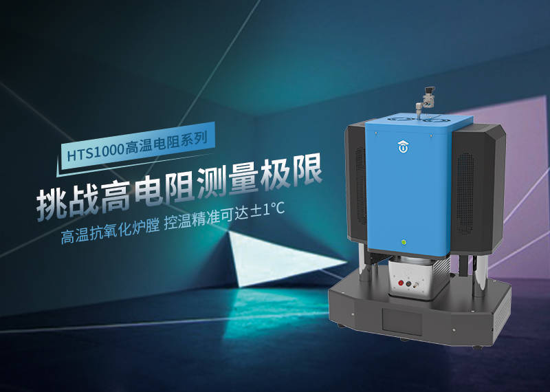
For testing across standard power electronic operational envelopes up to 800°C, the MatMeas HTS-1000HR high-temperature resistivity measurement system provides dedicated three-ring guarded metrology. To prevent fixture insulation breakdown from masking substrate properties, the HTS-1000HR incorporates structural components fabricated entirely from ultra-high-purity (99.8%) sintered corundum ceramics, ensuring that fixture isolation resistance exceeds 10^14 Ω even at 600°C. To protect delicate thin-film ceramic substrates from fracturing under thermal expansion, the system utilizes a calibrated micro-loading contact head that applies a constant, non-destructive contact pressure of just 0.25 N. Furthermore, an environmental chamber supports vacuum evacuation down to 10^-1 Pa and inert gas purging, completely preventing the oxidation of platinum, gold, or molybdenum electrodes.
For mission-critical applications operating in extreme thermal domains—such as deep-well geothermal logging sensors, aerospace turbine monitoring, and nuclear reactor instrumentation—characterization must extend far beyond 800°C. The MatMeas RMS-1650 ultra-high-temperature measurement system pushes characterization limits up to 1600°C. Featuring a heavy-duty muffle furnace with molybdenum disilicide (MoSi2) heating elements, multi-layer ceramic thermal shields, and active triaxial guarding, the RMS-1650 measures volume resistivity across sixteen orders of magnitude, providing the empirical foundation required for ultra-high-temperature packaging qualification.
Standardized Specimen Preparation and Electrification Protocols
- Electrode Geometry Precision: Circular electrodes should be applied using screen-printed, fired-on noble metal organometallic pastes (platinum or gold) or sputtering. Ensure that the annular guard gap
gis uniform within ±0.05 mm around the circumference. - Electrification Time Soak: In accordance with ASTM D257, allow a standardized electrification soak of 60 seconds at each discrete DC voltage step before recording resistance. This ensures that transient geometric capacitance charging and slow dielectric absorption currents decay below the steady-state leakage current.
- Thermal Equilibrium Dwell: During thermal stepping, enforce a minimum dwell time of 5 to 10 minutes at each setpoint, verifying that substrate temperature is stable within ±0.5°C to prevent thermoelectric Seebeck voltage offsets.
FAQ
Q: Why do generic high-temperature test fixtures produce wildly inaccurate resistance readings above 600°C?
A: At temperatures exceeding 600°C, standard ceramic and mica insulating materials used within generic test fixtures begin to suffer thermal carrier activation, causing their own internal electrical resistance to drop sharply. As a result, the measurement fixture creates a massive parallel parasitic leakage path to ground that completely masks the true volume resistance of the test substrate. Dedicated systems like the MatMeas HTS-1000HR utilize ultra-high-purity (99.8%) corundum insulation and driven guard architectures, ensuring that the fixture's internal resistance remains several orders of magnitude higher than the specimen.
Q: What is the physical distinction between volume resistivity and surface resistivity in ceramic packaging?
A: Volume resistivity (expressed in Ω·cm) measures the intrinsic electrical resistance to current flowing directly through the thickness of the ceramic substrate; it dictates the component's bulk dielectric breakdown and dielectric loss characteristics. Surface resistivity (expressed in Ω/sq) measures the resistance to current tracking along the exterior face of the ceramic; it is heavily influenced by ambient humidity, surface roughness, and ionic contaminants, dictating the minimum safe creepage distance between high-voltage conductor traces.
Q: How does the dual-polarity current reversal technique eliminate thermal voltage errors at 1000°C?
A: In high-temperature furnaces, even minor thermal gradients between the upper and lower electrode probes generate a parasitic DC voltage via the thermoelectric Seebeck effect. When measuring high-resistance materials where test currents are in the nanoampere or microampere regime, this Seebeck voltage induces severe measurement offsets or apparent "negative resistance." Applying current in the forward direction (V_forward), reversing the polarity (V_reverse), and computing V_true = (V_forward - V_reverse) / 2 completely cancels the thermal EMF baseline.
Related Instruments & Equipment
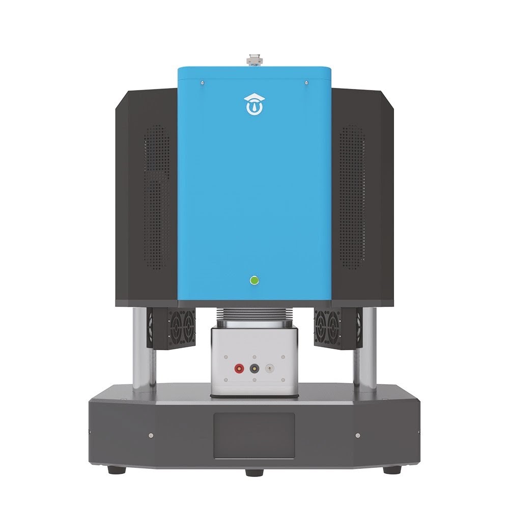
HTS1000HR High Temperature Resistivity Measurement System
The HTS1000HR is an advanced, integrated testing platform specifically engineered to precisely evaluate the electrical conductivity and insulation properties of advanced materials at extreme temperatures up to 800℃. By supporting various atmospheric conditions and offering an ultra-wide resistance measurement range, it serves as an indispensable characterization tool for material research and industrial quality control.
View details →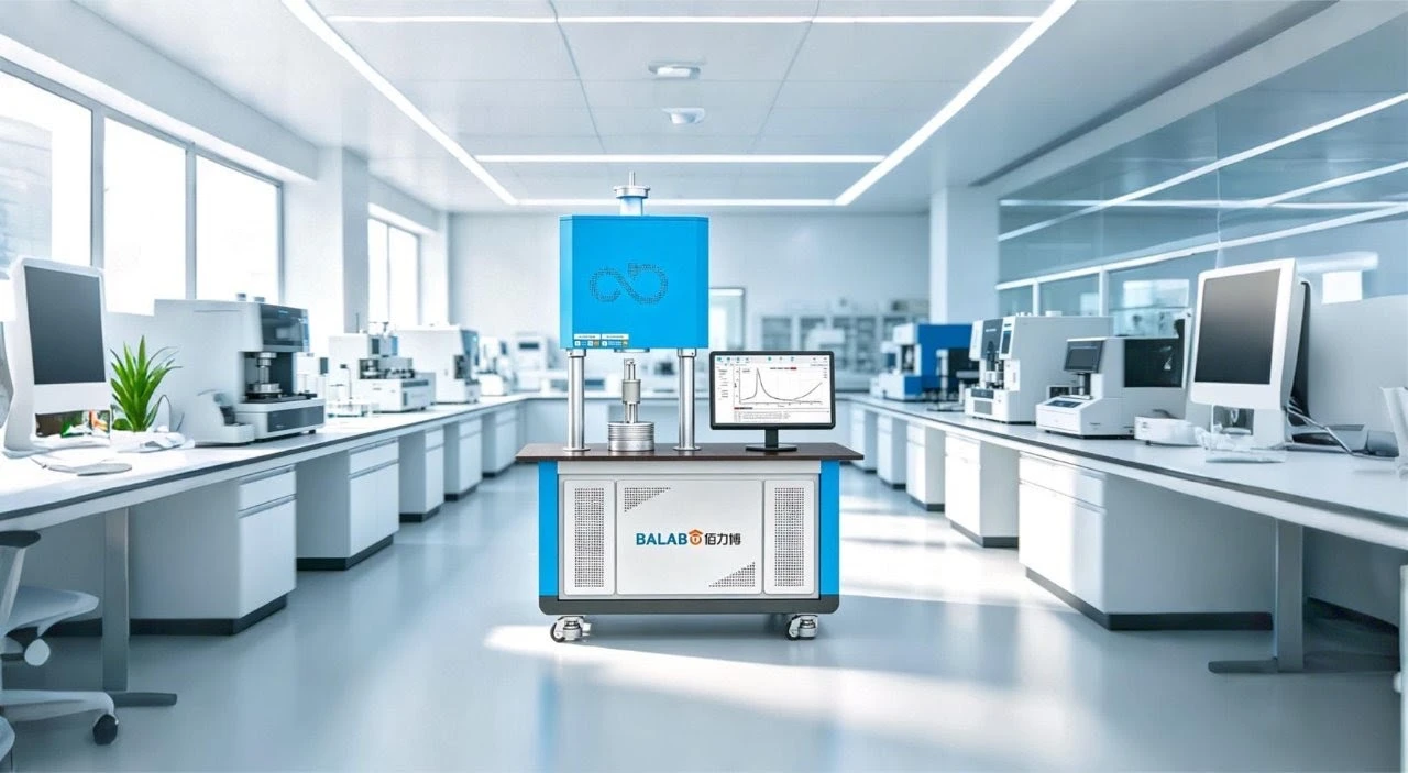
RMS1650 Ultra-High Temperature Resistivity Measurement System
The RMS1650 Ultra-High Temperature Resistivity Measurement System is engineered for the rigorous electrical characterization of insulating and dielectric materials up to 1600°C. Utilizing a proprietary guarded three-terminal electrode configuration, the system enables in-situ acquisition of resistivity and leakage current kinetics under extreme temperatures, vacuum, and controlled gas atmospheres.
View details →Request High-Precision Testing Solutions
Get expert guidance and customized instruments for your functional materials project.