High-Temperature Electrical Conductivity Testing of Metals and Alloys
Technical News
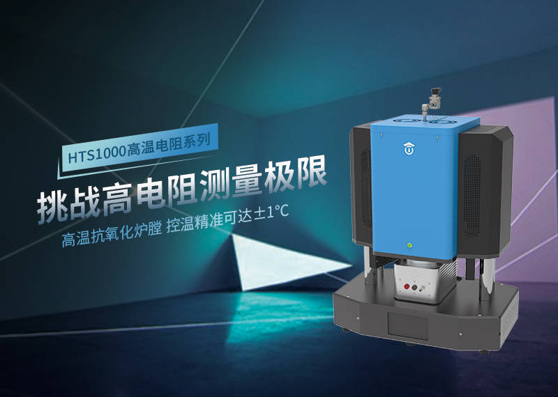
Electrical conductivity and its reciprocal, electrical resistivity, represent fundamental physical transport properties that dictate the operational efficiency, current-carrying capacity, and thermal stability of metallic conductors, structural alloys, and advanced refractory systems. In electric vehicle (EV) busbars, aerospace turbine instrumentation, power generation switchgear, and semiconductor lead frames, metallic components face severe thermal stresses where operational temperatures escalate from ambient to 600°C, 800°C, or well above 1000°C.
Characterizing metallic conductivity across wide thermal profiles provides crucial data for electrical engineers and metallurgists. Because resistivity in conductors can be as low as nano-ohms (nΩ), standard two-wire measurement techniques fail completely due to parasitic lead and contact resistances. Furthermore, measuring conductors at elevated temperatures introduces severe experimental hurdles: intense thermoelectric Seebeck voltages, violent open-air oxidation, and contact degradation. Overcoming these challenges requires standardized four-point probe and four-wire Kelvin metrology conforming to ASTM B193, ASTM E1004, and SEMI MF84 specifications.
Solid-State Physics of High-Temperature Metallic Conduction
In pure metals and conductive alloys, electrical conduction is mediated by free valence electrons drifting through a periodic crystalline ion lattice. According to Matthiessen's Rule, the total electrical resistivity ρ(T) is partitioned into independent scattering contributions:
ρ(T) = ρ_impurity + ρ_phonon(T)
- Residual Impurity Resistivity (ρ_impurity): Originates from electron scattering off static crystal lattice imperfections, grain boundaries, dislocations, and chemical solute atoms. In accordance with Nordheim's rule for disordered binary solid solutions,
ρ_impurityis independent of temperature, defining the residual resistivity at 0K. - Thermal Phonon Scattering (ρ_phonon(T)): As temperature increases, thermal kinetic energy amplifies the vibrational amplitude of lattice ions (phonons). Free electrons scatter with increasing frequency against these thermal lattice vibrations, shortening the mean free path
l_eand causing electrical resistivity to rise linearly with temperature above the Debye temperature (θ_D).
Across standard engineering temperature ranges, the temperature-dependent resistivity is modeled by the linear Temperature Coefficient of Resistance (TCR, denoted as α):
ρ(T) = ρ_0 * [ 1 + α * ( T - T_0 ) ]
where ρ_0 is the baseline resistivity measured at reference temperature T_0 (typically 20°C or 25°C), and α is the material TCR (expressed in 1/K or ppm/K).
For pure noble metals like copper and aluminum, α is positive and relatively high (~3.9 * 10^-3 / K to 4.3 * 10^-3 / K), meaning that electrical resistance nearly doubles between 25°C and 250°C. In contrast, specialized high-entropy alloys and nickel-chromium resistance alloys exhibit near-zero TCR due to intense baseline electron scattering off chemical disorder, maintaining stable resistance across wide thermal envelopes.
Contact Resistance Elimination: Four-Point Probe vs. Four-Wire Kelvin
When evaluating high-conductivity metals—where total specimen resistance routinely spans 1 µΩ down to 10 nΩ—traditional two-wire measurement introduces errors exceeding 1,000%. In a two-wire circuit, test leads and mechanical probe interfaces contribute contact resistances ranging from 10 mΩ to over 1 Ω, completely drowning out the intrinsic material resistance.
To decouple contact resistance from the specimen, standardized metrology deploys four-terminal configurations tailored to specimen geometry:
1. The Collinear Four-Point Probe Method (Thin Films & Sheets)
In thin metal foils, sputtered coatings, and semiconductor metallization layers, four equispaced collinear probes contact the specimen surface:
- Outer Probes (1 and 4): Deliver a controlled DC or low-frequency AC current
I. - Inner Probes (2 and 3): Connect to an ultra-high-input-impedance voltmeter (
Z_in > 10^12 Ω) to measure the potential dropΔV.
Because virtually zero current flows through the voltage sensing circuit, contact resistance and lead wire resistance across probes 2 and 3 drop zero potential, eliminating contact errors. For a thin conductive layer of thickness t where thickness is much smaller than probe spacing s (t << s), the sheet resistance R_s and bulk volume resistivity ρ are calculated per SEMI MF84:
R_s = [ π / ln(2) ] * ( ΔV / I ) * F_geom ≈ 4.5324 * ( ΔV / I ) * F_geom
ρ = R_s * t
where F_geom is a geometric correction factor accounting for specimen boundary proximity and finite sample dimensions.
2. The Four-Wire Kelvin Resistance Method (Bulk Bars & Rods)
For thick metal busbars, cast superalloys, and cylindrical rods, a four-wire Kelvin bridge arrangement is preferred. Current leads are clamped securely across the opposing end faces of the sample to ensure uniform current density streamlines through the cross-sectional area A. Separate potential pick-up knives or needle contacts measure the voltage drop ΔV across a defined gauge length L:
ρ = ( ΔV / I ) * ( A / L )
Conforming to ASTM B193, this method provides traceable, high-precision resistivity extraction across massive structural conductors.
| Conductor Material System | Compositional Specification | Resistivity @ 25°C (µΩ·cm) | Resistivity @ 300°C (µΩ·cm) | Resistivity @ 600°C (µΩ·cm) | Resistivity @ 1000°C (µΩ·cm) | Linear TCR α (10^-3 / K @ 25°C) | Thermal Conductivity @ 25°C (W/m·K) | High-Temperature Degradation Mechanism |
|---|---|---|---|---|---|---|---|---|
| OFHC Copper (C10100) | 99.99% pure oxygen-free copper | 1.71 | 3.55 | 5.80 | 9.20 | 3.93 | 398 | Severe oxidation in air >200°C; grain growth softening |
| 6061-T6 Aluminum Alloy | Al-1.0Mg-0.6Si structural alloy | 3.99 | 8.20 | 14.50 | Melts @ 652°C | 4.10 | 167 | Over-aging precipitate coarsening at >150°C |
| Inconel 718 Superalloy | Ni-19Cr-18.5Fe-5Nb-3Mo-0.9Al | 125.0 | 132.0 | 138.0 | 144.0 | 0.15 | 11.4 | High intrinsic resistance; γ'' precipitate phase stability |
| Ti-6Al-4V (Grade 5) | Alpha-beta structural titanium alloy | 178.0 | 185.0 | 192.0 | 200.0 | 0.12 | 6.7 | Interstitial oxygen/nitrogen embrittlement >500°C |
| Platinum (Pt Reference) | 99.999% high-purity reference metal | 10.6 | 21.2 | 31.8 | 44.5 | 3.92 | 71.6 | Highly stable; international thermometry benchmark |
| Tungsten (W Refractory) | 99.95% refractory sintered metal | 5.30 | 11.8 | 19.5 | 32.0 | 4.50 | 173 | Catastrophic oxidation in air >400°C; requires vacuum |
Overcoming High-Temperature Testing Hazards: Thermal EMF and Oxidation
Executing metallic conductivity measurements at temperatures up to 1000°C introduces severe experimental hazards that paralyze conventional low-resistance meters:
- Thermoelectric Seebeck Voltage (Thermal EMF): In high-temperature furnaces, even slight thermal gradients (e.g., 2°C) between the two voltage sensing junctions create a parasitic DC thermocouple voltage via the Seebeck effect. When testing low-resistance conductors where the true IR voltage drop
ΔVis only tens of microvolts, a 100 µV Seebeck EMF completely obliterates the measurement, often causing apparent "negative resistance." - Catastrophic Atmospheric Oxidation: Heating base metals (copper, aluminum, tungsten, or carbon conductors) in ambient air at temperatures above 300°C causes rapid surface oxidation. High-resistance oxide scales (such as CuO, Cu2O, or WO3) passivate the metal surface, destroying probe contact or eroding the conductor's active cross-section.
Pulsed Bipolar Current Reversal Protocol:
Forward Cycle:   V_meas(+) = I * R_true + V_Seebeck
Reverse Cycle:   V_meas(-) = -I * R_true + V_Seebeck
Cancellation:    V_true = [ V_meas(+) - V_meas(-) ] / 2 = I * R_true
Result:          Pure R_true Extracted; V_Seebeck Completely Eliminated
To eliminate thermal EMF, modern systems implement the Pulsed Bipolar Current Reversal Technique. The system injects a forward current pulse (+I), recording V_meas(+) = I * R_true + V_Seebeck. The polarity is then immediately reversed to -I, recording V_meas(-) = -I * R_true + V_Seebeck. By computing the algebraic difference:
V_true = [ V_meas(+) - V_meas(-) ] / 2
the thermal EMF baseline V_Seebeck is mathematically canceled, delivering sub-nanovolt measurement fidelity regardless of furnace thermal gradients.
| Conductivity Testing Methodology | Specimen Geometry & Format | Practical Resistance Dynamic Range | Contact Resistance Sensitivity | High-Temperature Atmospheric Limitation | Governing Standard |
|---|---|---|---|---|---|
| Collinear 4-Point Probe | Thin metallic foils, sputtered films, wafers | 0.1 mΩ/sq to 100 MΩ/sq | Mathematically eliminated via high-Z sensing | Vacuum / inert atmosphere required to prevent probe oxidation | SEMI MF84, ASTM F390 |
| 4-Wire Kelvin Bridge | Solid metal bars, cylindrical rods, busbars | 1 nΩ to 1 GΩ | Zero current in voltage sense leads | Sealed muffle tube with continuous argon purge | ASTM B193, GB/T 351 |
| Eddy-Current Method | Planar non-magnetic sheets, aerospace skins | 1% to 105% IACS conductivity | Non-contact (Zero contact resistance) | Temperature limited by sensor coil thermal limits (< 200°C) | ASTM E1004 |
Dedicated High-Temperature In-Situ Testing Systems
Achieving traceable conductivity characterization across broad temperature envelopes requires integrated systems pairing precision low-noise electronics with atmosphere-controlled thermal stages.
For thin metallic foils, conductive battery current collectors, and thin-film coatings, the MatMeas RMS-1000P high-temperature four-point probe resistivity system provides specialized metrology up to 1000°C. To protect delicate sub-micron films from mechanical puncturing, the RMS-1000P features a motorized z-axis loading stage that regulates probe contact force with micro-newton repeatability. Furthermore, it incorporates active electrostatic discharge (ESD) neutralization, preventing residual static charges from vaporizing thin films prior to mechanical contact.
For bulk structural components, conductive superalloys, and carbon materials, the MatMeas RTS-1000C high-temperature conductive material resistivity measurement system (upgraded generation of the RMS-1000C platform) provides four-wire Kelvin characterization from room temperature to 600°C (with extended thermal envelopes up to 1000°C). Featuring an integrated sealed quartz thermal environment capable of maintaining inert argon, nitrogen, or vacuum environments (< 10^-1 Pa), the RTS-1000C completely prevents oxidation of copper, refractory tungsten, and graphite specimens. Driven by closed-loop current reversal electronics, the RTS-1000C resolves resistances down to 10 nΩ, providing reliable high-temperature conductivity data for aerospace and power transmission engineering.
FAQ
Q: Why does the thermoelectric Seebeck effect distort nano-ohm resistance testing at 800°C?
A: When testing metallic conductors at elevated temperatures, slight temperature differences between the two contact probes create a thermal gradient across the junction of dissimilar metals (the test probe and the sample). This generates a parasitic DC thermoelectric voltage via the Seebeck effect that can easily reach tens or hundreds of microvolts. Because the actual resistive voltage drop across a highly conductive sample is often less than 10 microvolts, the Seebeck EMF completely swamps the measurement. The pulsed current reversal method implemented in the MatMeas RTS-1000C cancels this DC offset mathematically.
Q: What is the physical significance of the temperature coefficient of resistance (TCR)?
A: The temperature coefficient of resistance (TCR) quantifies the fractional rate of electrical resistivity change per degree of temperature shift. For pure conductors like copper, TCR is positive (~0.0039 / K), reflecting increased electron-phonon scattering as thermal lattice vibrations intensify. For electrical engineers, a high TCR requires significant current derating at high temperatures to avoid thermal runaway in EV power busbars and aerospace wiring harnesses.
Q: Why must thin-film four-point probe testing be conducted under high vacuum or inert purge?
A: At temperatures above 200°C to 300°C, pure metals like copper, nickel, and molybdenum react aggressively with atmospheric oxygen, forming thick, non-conductive oxide layers. In thin-film specimens where total film thickness is only a few hundred nanometers, air oxidation can consume the entire conductor layer within minutes. Conducting the test within a sealed vacuum or inert gas chamber, as featured on the MatMeas RMS-1000P, prevents chemical degradation and preserves electrical contact throughout the thermal cycle.
Related Instruments & Equipment
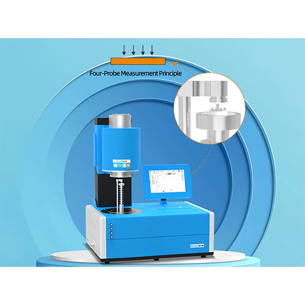
MatMeas RMS-1000P High-Temp Four-Point Probe Resistivity System
RMS-1000P uses four-point probe method for thin film and wafer resistivity measurement, featuring dual-electrostatic measurement, 0.1mΩ~100MΩ range, and specialized fixture for semiconductor materials.
View details →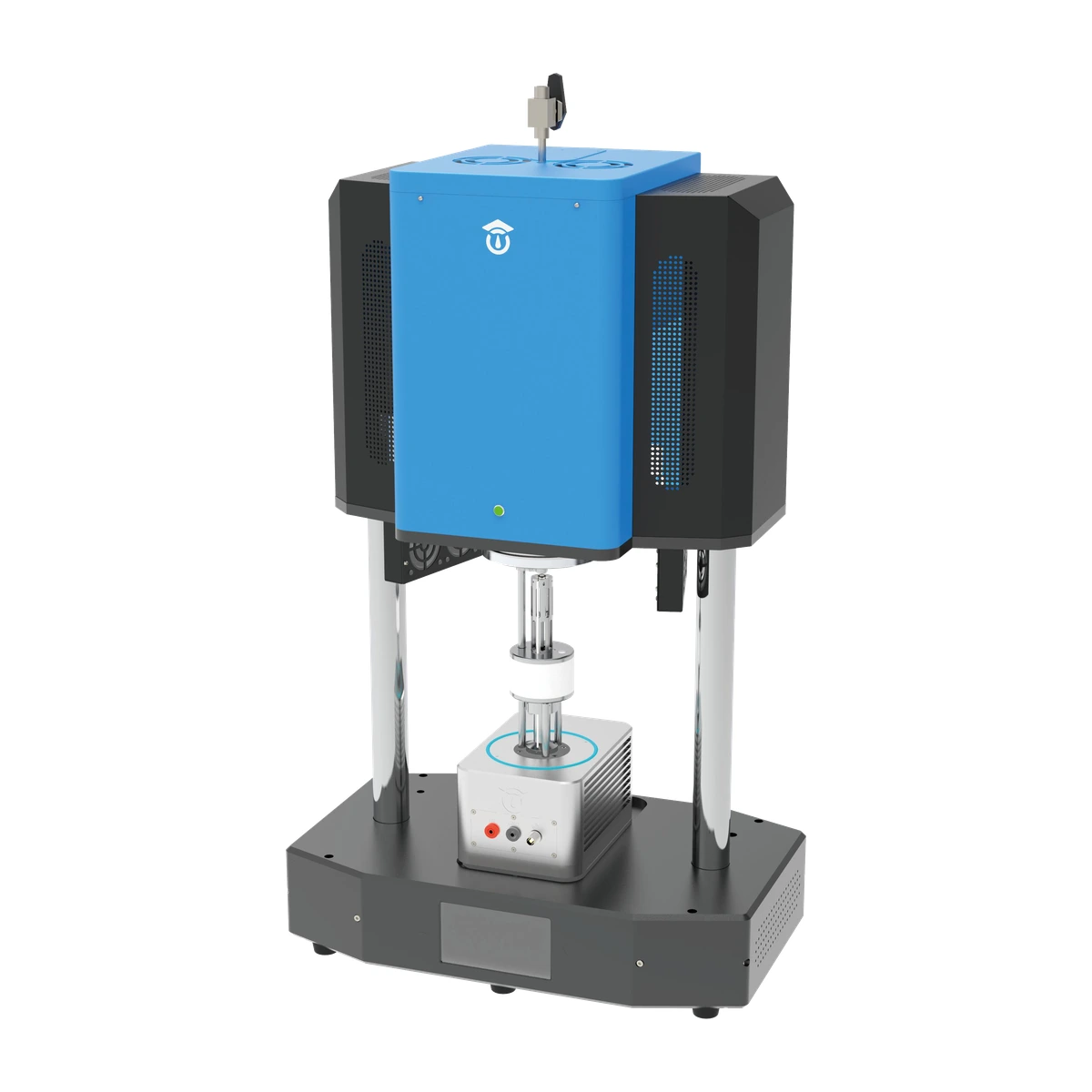
MatMeas RTS-1000C High-Temp Conductive Material Resistivity System (Upgraded from RMS-1000C)
The MatMeas RTS-1000C is the next-generation flagship evolution of the earlier RMS-1000C system, purpose-built for precision high-temperature conductive material resistivity measurement via four-wire Kelvin method. Delivering nΩ-to-MΩ resolution (10 nΩ to 100 MΩ) from RT to 600°C (standard, with optional package up to 1000°C under controlled N₂/Ar), the upgraded platform features 99% zirconia thermal isolation, a rigid motorized test stand, and hybrid platinum/tungsten-carbide probes for vacuum and controlled atmospheres.
View details →Request High-Precision Testing Solutions
Get expert guidance and customized instruments for your functional materials project.