Electrical Characterization of Multilayer Ceramic Capacitors
Technical News
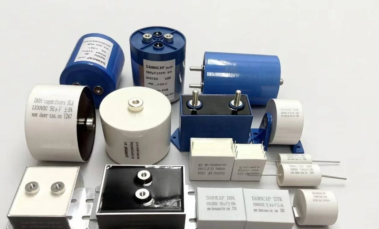
Multilayer Ceramic Capacitors (MLCCs) represent the highest-volume passive electronic components in modern microelectronics, with trillions of units deployed annually across automotive traction inverters (AEC-Q200 qualified), 5G smartphone motherboards, artificial intelligence accelerator power distribution networks (PDNs), and aerospace avionics. An MLCC consists of interleaved layers of dielectric ceramic tape (ranging from sub-micron thickness up to tens of micrometers) co-fired with alternating internal metal electrodes (primarily base-metal nickel, BME, or noble-metal silver-palladium) terminating at external copper-nickel-tin metallization bands.
Depending on dielectric formulation, MLCCs are bifurcated under EIA-198-D and IEC 60384 standards into Class I ultra-stable paraelectrics (such as titanium dioxide and neodymium titanate-based C0G/NP0) and Class II/III high-permittivity ferroelectrics (primarily doped barium titanate, BaTiO3, including X5R, X7R, X8R, and Y5V formulations). While Class II dielectrics provide massive volumetric capacitance (up to 100 uF in a single 0805 or 1206 package), their electrical performance is strongly non-linear, exhibiting steep dependencies on operating frequency, ambient temperature, AC test amplitude, applied DC bias field, and thermal aging history.
A defensible characterization program requires decomposing MLCC performance into small-signal broadband impedance spectra, non-linear DC bias voltage derating, and high-temperature accelerated lifetime degradation (HALT).
Frequency-Dependent Complex Impedance and the Parasitic Spectrum
In real-world circuit layouts, an MLCC does not behave as an ideal lumped capacitor. Interconnect geometry, internal electrode resistance, skin effect, and inductive current loops introduce parasitic elements modeled by the series RLC equivalent circuit:
Z*(omega) = ESR + j * [omega * ESL - 1 / (omega * C)]
+---------------------------------------------------------------------------------------------------+
|                        MLCC Complex Impedance vs Frequency Spectrum                               |
+---------------------------------------------------------------------------------------------------+
|   Impedance |Z| (Ohms)                                                                            |
|       ^                                                                                           |
|  10^3 |*** Capacitive Region                                                                      |
|       |   *****  |Z| approx 1 / (omega * C)                                                       |
|  10^0 |        *****                                                      ***** Inductive Region  |
|       |             *****                                            *****      |Z| approx omega*L|
| 10^-3 |                  *****       Self-Resonant Frequency (SRF)  *****                         |
|       |                       ****               v             *****                              |
|       |                           *             ***           *                                   |
|       +----------------------------+-----------*---*---------+-------------------------> Frequency|
|                                                |ESR|                                              |
|                                                \---/ Minimum Impedance                            |
+---------------------------------------------------------------------------------------------------+
The impedance profile is divided into three distinct operational regimes:
1. Capacitive Regime (f < f_SRF)
At low frequencies, the capacitive reactance (1 / (omega * C)) dominates the total impedance:
|Z(omega)| approx 1 / (2 * pi * f * C)
The phase angle (theta) resides near -90 degrees. In this band, the component stores and releases electrostatic energy, serving power decoupling, DC-blocking, and filtering functions.
2. Self-Resonant Frequency (f = f_SRF)
As excitation frequency rises, the inductive reactance of internal electrode interconnections (omega * ESL) increases linearly until it exactly balances the capacitive reactance:
omega_SRF * ESL = 1 / (omega_SRF * C)
The Self-Resonant Frequency (f_SRF) is given by:
f_SRF = 1 / (2 * pi * sqrt(ESL * C))
At f_SRF, net reactance cancels to zero (phase angle theta = 0 degrees), and the impedance collapses to its absolute minimum value, which defines the Equivalent Series Resistance (ESR):
|Z|_min = ESR
In high-speed power distribution networks (PDN), decoupling capacitors are sized so that their f_SRF coincides with microprocessor clock switching harmonics, providing a low-impedance shunt to ground.
3. Inductive Regime (f > f_SRF)
Above f_SRF, the inductive reactance outpaces capacitive impedance:
|Z(omega)| approx 2 * pi * f * ESL
The phase angle shifts to +90 degrees, and the MLCC behaves as an inductor. Attempting to filter high-frequency noise above f_SRF increases power bus ripple. To minimize ESL, capacitor manufacturers utilize reverse-geometry terminations (e.g., 0306 instead of 0603 packaging) and interdigitated low-inductance capacitor (LLC) designs.
Non-Linear DC Bias Derating in Class II Ferroelectric MLCCs
The most severe operational trap in MLCC circuit design is the DC bias effect. In Class II barium titanate dielectrics, ferroelectric domains switch spontaneously to minimize crystal energy. When an external DC bias voltage (V_DC) is superimposed across the capacitor terminals, an internal DC electric field (E_DC = V_DC / d_layer) aligns ferroelectric dipoles parallel to the applied field.
As the internal field increases, ferroelectric domain wall mobility freezes, saturating the polarizable dipole capacity of the crystal lattice. Under intense DC fields, the apparent small-signal capacitance plummets by 40% to over 80% of its rated nominal value:
Delta C(V_DC) / C_0 approx - alpha_bias * E_DC^2 = - alpha_bias * (V_DC / d_layer)^2
Capacitance Retention vs DC Bias Field:

Capacitance (% of Nominal)
   100% |======================== Class I (C0G/NP0): 100% Flat (Zero Bias Drop)
        |
        |-------\
    50% |        \------------ Class II (X7R): Smooth 30-50% Drop
        |                     \
        |                      \-------\
     0% +-------------------------------\================= Class III (Y5V): Severe 80-90% Drop
        0                               20                                50
                              Applied DC Bias Field (V/um)
Because modern sub-micron MLCCs utilize active ceramic layers as thin as 0.8 um, applying a rated voltage of merely 10 V generates an electric field of 12.5 V/um (125 kV/cm). Circuit engineers unaware of this phenomenon often discover that a 10 uF X7R output filter drops to 2.2 uF under full operating load, inducing power supply instability.
Dielectric Classification Matrix: Standards and Performance Boundaries
The table below compiles EIA-198-D and IEC 60384 standards governing temperature stability, aging rates, and DC bias sensitivity across MLCC dielectric classes.
| EIA Dielectric Class Code | Operating Temperature Window | Maximum Capacitance Drift (Delta C / C_0) | Dielectric Base Material System | DC Bias Voltage Sensitivity | Typical Aging Rate (% per decade) | Primary Circuit Function |
|---|---|---|---|---|---|---|
| Class I: C0G / NP0 | -55 C to +125 C | 0 +/- 30 ppm/K (+/-0.54% max) | Paraelectric Nd2Ti2O7 / CaZrO3 | Zero; completely invariant to DC bias | 0.0% (Zero aging; no ferroelectric decay) | Precision RF tuning, resonant tanks, high-Q timing |
| Class II: X5R | -55 C to +85 C | +/-15% across temperature | Doped BaTiO3 with fine grain (sub-micron) | Moderate to high (drops 30% to 70% at rated V) | 1.5% to 2.5% per decade hour | Consumer mobile decoupling, bypass filtering |
| Class II: X7R | -55 C to +125 C | +/-15% across temperature | Core-shell BaTiO3 + rare-earth dopants | Moderate (drops 20% to 60% at rated V) | 1.0% to 2.0% per decade hour | Industrial and automotive (AEC-Q200) decoupling |
| Class II: X8R | -55 C to +150 C | +/-15% across temperature | Heavily engineered BaTiO3-BiMeO3 | Moderate (drops 20% to 50% at rated V) | 1.0% to 1.8% per decade hour | Under-the-hood automotive engine controllers |
| Class III: Y5V | -30 C to +85 C | +22% / -82% (extreme drift) | High-permittivity BaTiO3 (Curie near 25 C) | Severe (drops 70% to 90% at rated V) | 3.0% to 5.0% per decade hour | Low-cost non-critical bulk decoupling |
Logarithmic Aging and De-Aging Kinetics
Class II ferroelectric ceramics undergo a continuous, spontaneous reduction in capacitance and dielectric loss over time, known as dielectric aging. Following sintering and subsequent cooling through the Curie temperature (T_c approx 120 C for BaTiO3), ferroelectric domains nucleate in high-energy configurations. Over time, point defects and domain walls relax into lower-energy pinned configurations.
The aging process conforms strictly to a logarithmic time decay:
C(t) = C(t_0) * [1 - (A_rate / 100) * log10(t / t_0)]
Where A_rate is the aging rate expressed in percent per decade hour:
A_rate = - [ (C(t_2) - C(t_1)) / C(t_1) ] / [ log10(t_2 / t_1) ] * 100%
To reset the aging clock and establish a repeatable baseline for capacitance qualification, specimens must undergo De-Aging: heating the MLCC to 150 C (well above T_c) for 60 minutes, followed by controlled cooling to room temperature. Capacitance measurements are then logged exactly 24 hours post-de-aging.
Four-Terminal-Pair (4TP) Kelvin Measurement Architecture
Measuring high-capacitance MLCCs (1 uF to 100 uF) and ultra-low ESR values (sub-10 milliohms) requires eliminating test lead and contact resistance. Standard two-terminal fixtures introduce lead resistance (typically 50 to 200 milliohms) that dwarfs the true ESR of the capacitor.
+---------------------------------------------------------------------------------------------------+
|                        Four-Terminal-Pair (4TP) Kelvin Test Architecture                          |
+---------------------------------------------------------------------------------------------------+
|                                                                                                   |
|  Current Drive High (H_cur) -----------------------------+                                        |
|                                                          |                                        |
|  Voltage Sense High (H_pot) -----------------------+     |                                        |
|                                                    |     |                                        |
|                                                  +-v-----v-+                                      |
|                                                  |   DUT   | MLCC Device Under Test               |
|                                                  +-^-----^-+                                      |
|                                                    |     |                                        |
|  Voltage Sense Low (L_pot) ------------------------+     |                                        |
|                                                          |                                        |
|  Current Drive Low (L_cur) ------------------------------+                                        |
|                                                                                                   |
|  Outer Coaxial Shields: Tied together at terminal plane to eliminate mutual inductive coupling   |
+---------------------------------------------------------------------------------------------------+
The table below outlines four-terminal-pair (4TP) calibration techniques and parasitic compensation methods.
| Measurement Challenge | Physical Root Cause | Impact on MLCC Measurement | Engineering Mitigation Protocol |
|---|---|---|---|
| Contact Resistance (R_contact) | Mechanical pressure variation on component termination bands | Artificially inflates measured ESR by 10 to 100 milliohms | Utilize gold-plated Kelvin tweezers; execute 4TP separate force/sense |
| Lead Inductance (L_lead) | Wire loops between instrument front-end and component | Shifts measured f_SRF downward; distorts high-frequency phase | Execute Short calibration using zero-inductance copper shorting bar |
| Mutual Inductive Loop Coupling | AC drive currents in H_cur induce false voltages in H_pot loop | Severe ESR measurement distortion above 100 kHz | Maintain coaxial shielding up to the contact tips; tie outer shields |
| DC Bias High-Voltage Isolation | Applying high DC bias voltages directly to impedance bridge | Damages internal bridge circuitry; distorts AC sensing | Integrate high-voltage blocking capacitors and DC-feed chokes |
| Cable Parasitic Capacitance | High-impedance low-frequency testing of small Class I MLCCs | Shunts measured current, underestimating dissipation factor | Execute Open calibration with contacts positioned at exact test spacing |
The true impedance of the device under test (DUT) is isolated:
Z_DUT = (V_H_pot - V_L_pot) / I_H_cur
High-Acceleration Life Testing (HALT) and Reliability Physics
In automotive and industrial qualification (AEC-Q200), MLCCs undergo High-Acceleration Life Testing (HALT) to predict mean time to failure (MTTF) under thermal and electrical overdrive conditions. The primary long-term failure mechanism in BaTiO3 MLCCs is the electromigration of positively charged oxygen vacancies (V_O_ddot) under sustained DC electric fields:
V_O_ddot migrates toward the cathode (negative electrode), piling up at the dielectric-metal interface. This space-charge accumulation lowers the Schottky barrier height, accelerating electron injection and precipitating thermal runaway.
The Acceleration Factor (AF) linking accelerated test conditions to operational conditions is governed by the empirical Eyring-Arrhenius model:
AF = (V_stress / V_use)^n * exp[ (E_a / k_B) * (1 / T_use - 1 / T_stress) ]
Where:
- V_stress / V_use: Ratio of accelerated test voltage to nominal operating voltage (typically 2x to 4x rated voltage).
- n: Voltage acceleration exponent (typically n = 2.5 to 3.5 for BaTiO3 BME capacitors).
- E_a: Thermal activation energy for oxygen vacancy migration (typically 1.1 eV to 1.5 eV).
- k_B: Boltzmann constant (8.617e-5 eV/K).
- T_stress / T_use: Absolute temperatures in Kelvin.
Executing HALT at 140 C and 3x rated voltage accelerates failure kinetics by factors exceeding 1,000x, allowing reliability engineers to verify automotive 15-year mission profiles in 100 hours of laboratory testing.
Comprehensive Environmental and Dielectric Metrology Platforms
Accurate qualification of high-reliability MLCCs requires continuous environmental control across cryogenic, ambient, and extreme thermal conditions.
For high-temperature power electronics screening, downhole drilling modules, and DC-bias dielectric characterization up to 1000 C, the MatMeas DMS-1000 High-Temperature Dielectric Spectrometer provides four-sample automated multiplexing, allowing rapid comparative screening of MLCC batches under controlled inert, vacuum, or oxidizing atmospheres.
For automotive AEC-Q200 qualification and aerospace sub-zero testing (-55 C to +150 C and beyond), the MatMeas DMS-2000 High-Low Temperature Dielectric Spectrometer combines an automated liquid nitrogen cryostat with a high-vacuum chamber (-160 C to 450 C). Its vacuum enclosure completely eliminates atmospheric moisture condensation and frost formation near 0 C, guaranteeing pristine dielectric loss tangent measurements across continuous temperature ramps.
When conducting failure analysis on unencapsulated MLCC green-state chips, cross-sectioned micro-electrodes, or localized internal layers, the MatMeas CPS-7000 Cryogenic Vacuum Probe Station provides four-axis micromanipulated probing with pneumatic vibration damping, ensuring continuous, damage-free contact across rapid thermal sweeps.
Best-Practice Laboratory SOP for MLCC Electrical Characterization
To obtain audit-compliant, reproducible MLCC qualification data:
- Pre-Test De-Aging Conditioning:
- For Class II dielectrics (X5R, X7R, Y5V), heat capacitors in a clean lab oven to 150 C (+/-5 C) for 60 minutes.
- Cool naturally to 25 C in a controlled desiccator (<20% RH).
- Maintain a standardized post-de-aging stabilization dwell of exactly 24.0 hours before recording baseline capacitance.
- Four-Terminal-Pair (4TP) Fixture Calibration:
- Connect Kelvin test tweezers or test fixture to the impedance analyzer.
- Perform Open Calibration with fixture tips separated by the exact package length (e.g., 2.0 mm for 0805).
- Perform Short Calibration using a solid gold-plated copper shorting bar matching component dimensions.
- Small-Signal Capacitance and Loss Verification:
- Set AC test excitation amplitude to 1.0 V RMS (+/-0.2 V) at 1.0 kHz for C <= 10 uF, or 0.5 V RMS at 120 Hz for C > 10 uF, in accordance with IEC 60384-1.
- Record capacitance (C_p) and dissipation factor (tan delta / DF).
- DC Bias Voltage Derating Profile:
- Connect an isolated high-voltage DC bias adapter.
- Step DC voltage from 0 V to 150% of rated working voltage in discrete 10% increments.
- Dwell for 5 seconds at each voltage step to allow domain relaxation before logging small-signal capacitance.
- Broadband Impedance and Resonance Sweep:
- Sweep frequency logarithmically from 100 Hz to 30 MHz (or higher with RF-IV instruments).
- Identify series self-resonant frequency (f_SRF) and extract Equivalent Series Resistance (ESR = |Z|_min) and Equivalent Series Inductance (ESL = 1 / (4 * pi^2 * f_SRF^2 * C)).
- Insulation Resistance (IR) Verification:
- Apply 100% rated DC working voltage across capacitor terminals through a 1-kiloohm current-limiting resistor.
- Log insulation resistance after exactly 60 seconds of electrification at 25 C. Confirm that the RC product (R_insulation * C_nominal) exceeds 500 ohm-farads (or 10 gigaohms, whichever is lower).
Frequently Asked Questions (FAQ)
Why does the capacitance of a Class II MLCC increase slightly when test AC voltage is increased from 0.1 V to 1.0 V?
In ferroelectric barium titanate, domain walls reside in shallow potential energy wells formed by crystalline lattice defects. A tiny AC excitation voltage (0.1 V RMS) is insufficient to overcome pinning barriers, exciting only reversible intra-well lattice vibrations. Increasing the AC test amplitude to 1.0 V RMS provides sufficient mechanical-electrical energy to drive extrinsic, non-linear domain wall oscillations across potential barriers. This extrinsic domain wall motion adds a large polarization component that increases measured capacitance by 5% to 20%. International standards strictly fix AC test voltage (typically 1.0 V RMS for standard values and 0.5 V RMS for ultra-high capacitances) to ensure cross-manufacturer consistency.
What is the physical distinction between dissipation factor (DF) and Equivalent Series Resistance (ESR)?
Dissipation factor (DF, or tan delta) is the dimensionless ratio of active power dissipated to reactive power stored in the capacitor: DF = tan delta = R_series * omega * C. ESR is the physical real-part resistance (in ohms) of the capacitor at a given frequency, incorporating internal metal electrode resistance, lead termination resistance, and dielectric loss:
ESR = (tan delta) / (omega * C) = R_metal + [tan(delta_d) / (omega * C)]
At low frequencies, ESR is dominated by dielectric loss and scales inversely with frequency. Near self-resonance, dielectric reactance cancels out, and ESR reaches a minimum determined entirely by the ohmic resistance of the metal internal electrode layers.
Why do Class I C0G capacitors exhibit zero aging while Class II X7R capacitors degrade over time?
Class I C0G/NP0 capacitors are fabricated from paraelectric ceramics (such as neodymium titanate or calcium zirconate) whose centrosymmetric crystal lattice possesses zero spontaneous ferroelectric polarization and zero ferroelectric domains. Without domains, no domain wall pinning or defect relaxation can occur, resulting in an aging rate of exactly 0.00% per decade. In contrast, Class II X7R capacitors utilize tetragonal ferroelectric barium titanate, which possesses spontaneous domains. The gradual, post-cooling relaxation of domain walls into lower-energy pinned configurations continuously lowers polarizability, producing a measurable 1% to 2% logarithmic loss of capacitance per decade hour.
Related Instruments & Equipment
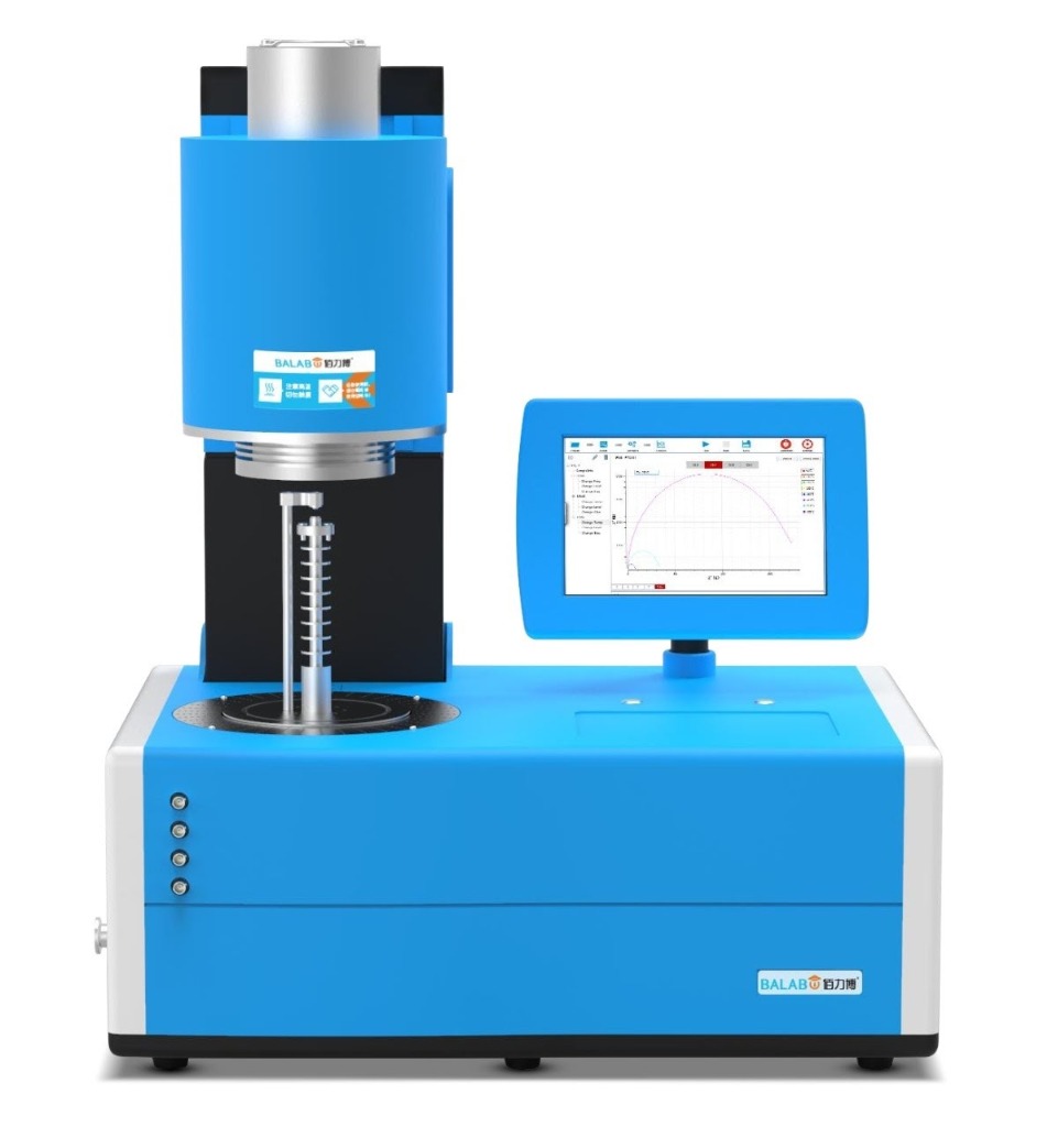
MatMeas DMS1000 High-Temperature Dielectric Spectrometer
The MatMeas DMS1000 is an advanced High-Temperature Dielectric Impedance Temperature Spectrometer engineered for the ultimate electrical characterization of bulk materials. Delivering an exceptional measurement accuracy of 0.05%, it operates efficiently from Room Temperature (RT) to 1000°C. Its upgraded platform supports both single-sample and four-sample simultaneous measurements. Integrated with a sealable metal shielding system and high-purity platinum electrodes, the DMS1000 enables highly reliable testing across inert, oxidizing, reducing, and vacuum atmospheres, making it an indispensable infrastructure for precision materials science.
View details →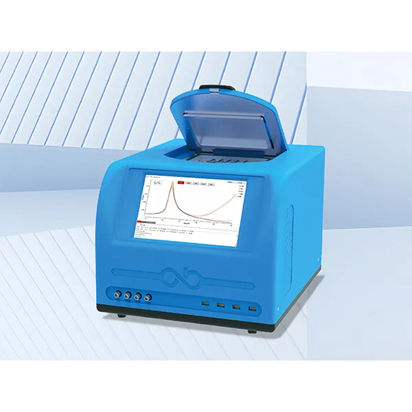
MatMeas DMS2000 High-Low Temperature Dielectric Spectrometer
The MatMeas DMS2000 is an advanced High and Low Temperature Dielectric Impedance Spectrometer engineered for evaluating the dielectric properties of materials under extreme thermal conditions. Compliant with the ASTM D150 standard, it integrates a proprietary LNP-95 liquid nitrogen injection system to achieve seamless continuous temperature variation from -160°C to 450°C. Uniquely featuring a vacuum-enabled sample chamber to completely prevent thermal frosting and eliminate false water peaks near 0°C, along with versatile options for single-sample or five-sample simultaneous testing, the DMS2000 ensures unparalleled data fidelity and high throughput for advanced scientific research.
View details →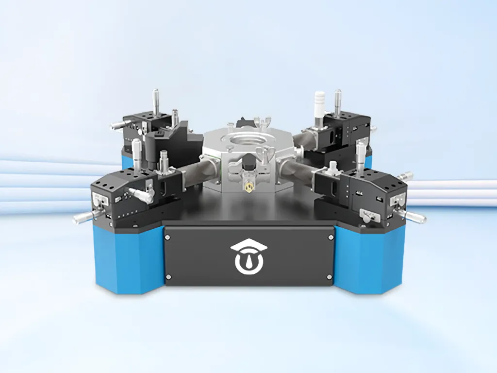
CPS7000 High-Low Temperature Dielectric Vacuum Probe Station
The MatMeas CPS7000 is an advanced, highly integrated desktop High-Low Temperature Dielectric Vacuum Probe Station engineered for the rigorous electrical characterization of thin films, bulk materials, and semiconductor wafers. Delivering performance directly comparable to industry-leading American brands like Lake Shore and Janis, this compact platform offers an ultra-wide temperature range from -160°C to 450°C via liquid nitrogen cooling. Uniquely equipped with a proprietary built-in air shock anti-vibration system, the CPS7000 eliminates data jumping points during continuous temperature variations. Supporting complex high-voltage and low-current testing environments, it is the ultimate infrastructure for evaluating dielectric, piezoelectric, ferroelectric, and TSDC properties in high-vacuum conditions.
View details →Request High-Precision Testing Solutions
Get expert guidance and customized instruments for your functional materials project.