Alumina Ceramic Low Temperature Resistivity Testing
Technical News
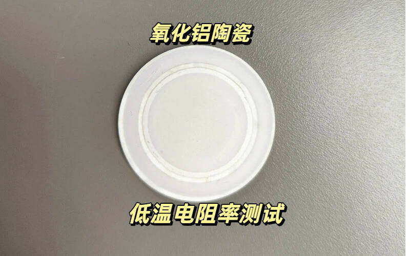
Polycrystalline alumina (Al2O3) ceramics serve as the premier electrical insulation and structural carrier platform across high-power electronics, RF telecommunications, and advanced aerospace packaging. While the elevated-temperature behavior of alumina is extensively documented for power electronic modules, modern electronic systems increasingly operate in severe sub-zero and deep cryogenic environments. Key applications include satellite instrumentation in deep-space trajectories, focal plane arrays in infrared space telescopes, superconducting quantum computing interconnects (4K to 77K), and magnetic levitation power electronics operating near liquid nitrogen temperatures (-196°C).
In these severe cryogenic regimes, assessing the electrical insulation reliability of alumina ceramics demands specialized metrological frameworks. While intrinsic volume resistivity climbs to extreme magnitudes (> 10^15 to 10^17 Ω·cm) as thermal lattice vibrations subside and charge carriers freeze out, thermomechanical mismatch stress between the ceramic substrate and bonded copper/gold metallization escalates drastically. Accurately testing low-temperature resistivity—free from frost-induced surface shunt leakage, triboelectric cable interference, and micro-cracking artifacts—is vital to guaranteeing the operational survivability of mission-critical cryogenic hardware.
Physics of Cryogenic Conduction: Carrier Freeze-Out and Mott Hopping
At temperatures above 300°C, electrical conduction in alumina is dominated by thermally activated oxygen vacancy migration and intergranular alkali ion drift through amorphous silicate boundary phases, following classical Arrhenius kinetics. As the temperature drops from ambient (298K) into sub-zero (-55°C / 218K) and cryogenic domains (77K liquid nitrogen down to 4K liquid helium), intrinsic band-to-band excitation and extrinsic vacancy hopping cease completely—a physical state known as carrier freeze-out.
Under deep cryogenic conditions, the negligible free carrier density means that any residual electronic transport across the bandgap (Eg ≈ 8.8 eV in high-purity α-Al2O3) occurs purely via quantum-mechanical tunneling between localized defect states. This transport mechanism is modeled by Mott's law of Variable-Range Hopping (VRH):
σ(T) = σ_0 * exp[ - ( T_0 / T )^(1/4) ]
where σ(T) is the electrical conductivity, σ_0 is the limiting conductivity pre-factor, T is absolute temperature in Kelvin, and T_0 represents Mott's characteristic temperature:
T_0 = 18 / [ k_B * N(E_F) * a^3 ]
Here, k_B is the Boltzmann constant (8.617 * 10^-5 eV/K), N(E_F) is the density of localized states near the Fermi energy level, and a is the spatial localization decay length of the wave function (typically a few angstroms).
Because conductivity falls exponentially with T^(-1/4), the volume resistivity of pure alumina exceeds 10^16 Ω·cm at 77K. In this regime, measuring electrical transport transitions from characterizing bulk material conduction to detecting microscopic dielectric anomalies, sub-surface pores, and surface leakage paths.
Thermomechanical Mismatch and Cryogenic Cracking Failure Modes
Although alumina's intrinsic bulk insulation improves at lower temperatures, the physical reliability of the overall ceramic assembly faces severe risks from differential thermal contraction. In direct bonded copper (DBC) and active metal brazed (AMB) ceramic circuit boards, the ceramic substrate is bonded to thick metallic conductors:
- Alumina Coefficient of Thermal Expansion (CTE): ~5.5 * 10^-6 / K to 7.0 * 10^-6 / K at room temperature, decreasing to ~1.2 * 10^-6 / K at 77K.
- Copper CTE: ~16.5 * 10^-6 / K at room temperature, maintaining ~10.0 * 10^-6 / K down to 77K.
Cooling from ambient down to -55°C or 77K induces severe interfacial shear stresses along the metal-ceramic boundary:
τ_max ≈ Δα * ΔT * G_metal * sqrt( d_metal / h_inter )
where Δα is the CTE mismatch, ΔT is the thermal drop, G_metal is the shear modulus of the metallization, d_metal is conductor thickness, and h_inter is the joint interlayer thickness.
If the interfacial shear stress exceeds the Griffith fracture toughness of the alumina matrix, sub-surface conchoidal micro-fissures propagate beneath the metallized pads. In ambient or partially sealed environments, trace atmospheric moisture is drawn into these micro-cracks via capillary action. Upon subsequent bias voltage application, these moisture-filled cracks generate intense localized electric fields, triggering catastrophic surface tracking breakdown and permanent insulation collapse.
| Ceramic Substrate System | Purity / Microstructure | Volume Resistivity @ 298K (Ω·cm) | Volume Resistivity @ 150K (Ω·cm) | Volume Resistivity @ 77K (Ω·cm) | Mean CTE (77K-298K, 10^-6 / K) | Thermal Conductivity @ 77K (W/m·K) | Dielectric Breakdown Field @ 77K (kV/mm) |
|---|---|---|---|---|---|---|---|
| 96% Al2O3 (Electronic Grade) | Polycrystalline with 4% silicate glass | 1.0 * 10^14 | 4.5 * 10^15 | > 1.0 * 10^16 | 4.8 - 5.2 | 85 - 110 | 18 - 22 |
| 99.6% Al2O3 (Laser Thin-Film) | Low-flux, high-purity α-alumina | 8.0 * 10^14 | > 1.0 * 10^16 | > 1.0 * 10^17 | 4.5 - 4.9 | 140 - 180 | 25 - 32 |
| AlN (Aluminum Nitride) | High thermal conductivity matrix | 2.0 * 10^14 | 8.0 * 10^15 | > 1.0 * 10^16 | 3.1 - 3.6 | 450 - 650 | 20 - 26 |
| Si3N4 (Silicon Nitride) | High-toughness AMB power grade | 3.0 * 10^14 | 1.2 * 10^16 | > 1.0 * 10^17 | 1.8 - 2.4 | 120 - 160 | 30 - 38 |
| ZTA (Zirconia Toughened Alumina) | 80% Al2O3 + 20% ZrO2 matrix | 5.0 * 10^13 | 1.0 * 10^15 | 8.0 * 10^15 | 6.2 - 6.8 | 45 - 65 | 16 - 20 |
Metrological Challenges: Surface Frost and Femtoampere Leakage
Measuring electrical resistances exceeding 10^13 to 10^15 Ω at cryogenic temperatures introduces extreme metrological challenges that render conventional benchtop test fixtures entirely ineffective:
- Atmospheric Moisture Condensation (Frost Bridging): When an unsealed test chamber drops below 0°C, ambient humidity condenses and freezes into a continuous frost layer across the ceramic surface. The surface conductivity of ice and liquid water bypasses the bulk ceramic, causing apparent volume resistivity to plummet by six orders of magnitude.
- Triboelectric and Piezoelectric Cable Noise: Flexible coaxial test cables undergo friction between inner dielectric layers and outer braid shields during mechanical vibration or thermal contraction, generating spurious triboelectric charges of 10 pC to 100 pC that overwhelm sub-picoampere signals.
- Electrode Mechanical Bounce: As thermal contraction shrinks micro-probe arms, mechanical tip contact can lift slightly off ceramic metallization pads, introducing noisy open-circuit oscillations during thermal sweeps.
| Cryogenic Test Artifact | Underlying Physical Origin | Impact on Measured Resistivity | Metrological Mitigation Protocol |
|---|---|---|---|
| Frost Condensation | Ambient water vapor freezing on substrate | Severe artificial drop in surface and volume resistivity | Evacuation to high vacuum (< 10^-2 Pa) prior to cooling |
| Triboelectric Cable Noise | Frictional charge generation from flexing cables | Fluctuating current baseline; false dielectric noise | Rigid semi-rigid triaxial cabling; active driven guard |
| Probe Micro-Slip | Differential thermal contraction of probe arms | Intermittent contact open-circuits; micro-arcing | Pneumatically isolated, spring-compliant probing tips |
| Dielectric Absorption Delay | Dipolar polarization currents during step voltage | Measured resistance drifts over hours | Standardized 60-second electrification soak time (ASTM D257) |
| Guard Shunt Overload | Surface leakage shunted to ground without isolation | Ground loop errors; electrometer amplifier saturation | Three-ring guarded electrode geometry with unity-gain buffer |
Precision Cryogenic In-Situ Testing via Vacuum Micro-Probing
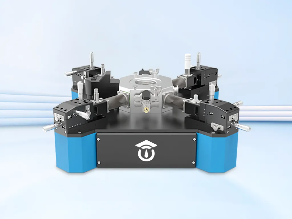
To eliminate condensation and mechanical instability during cryogenic characterization, advanced testing architectures integrate high-vacuum sample isolation with active vibration mitigation. The MatMeas CPS-7000 high-low temperature dielectric vacuum probe station addresses these environmental constraints by enclosing the testing stage within an evacuable chamber capable of sustaining vacuums below 10^-2 Pa. By maintaining a deep vacuum prior to introducing liquid nitrogen coolant, moisture condensation is completely prevented, enabling artifact-free resistivity profiling from -160°C up to 450°C.
To overcome mechanical probe dislodgement caused by thermal contraction during rapid temperature sweeps, the MatMeas CPS-7000 incorporates an integrated pneumatic shock-absorption and vibration isolation system directly within the chassis. Four independently manipulated micro-probing arms deploy specialized spring-loaded, low-thermal-mass tungsten tips. This architecture maintains constant contact pressure (< 0.2 N) across metallized alumina pads, preventing micro-scratching or contact loss throughout multi-hour thermal ramps.
In strict accordance with ASTM D257 and IEC 60093, true volume resistivity is separated from parasitic surface leakage via concentric three-terminal guard ring electrode geometry:
A_eff = (π / 4) * (d1 + g)^2
ρ_v = R_v * ( A_eff / t )
where d1 is the central electrode diameter, g is the annular guard gap, R_v is the measured volume resistance, and t is substrate thickness. By driving the concentric guard ring at an identical potential to the central measurement electrode, surface leakage currents are shunted directly to ground, ensuring that the central picoammeter captures only pure intrinsic bulk volumetric conduction.
Best Practices for Cryogenic Specimen Preparation
- Ultrasonic Degreasing and Vacuum Bake-Out: Substrates must undergo sequential ultrasonic degreasing in acetone and isopropanol, followed by a vacuum bake-out at 150°C for 60 minutes to desorb surface-bound hydroxyl groups before cryogenic testing.
- Metallization Integrity: Sputtered platinum or gold electrodes (100 nm to 200 nm thick with a 10 nm Ti or Cr adhesion layer) should be utilized to prevent electrode oxidation and thermal flaking under cyclic thermal shock.
- Voltage Electrification Soak: In compliance with ASTM D257, allow a minimum electrification soak time of 60 seconds at each discrete DC voltage step (typically 100 V to 500 V) to allow transient capacitive charging currents to decay below the system noise floor before recording resistance.
FAQ
Q: Why does volume resistivity increase at low temperatures while mechanical reliability decreases?
A: At low temperatures, thermally activated electron and ion hopping mechanisms freeze out, and intrinsic carrier concentration falls exponentially, driving bulk volume resistivity to extreme levels (> 10^16 Ω·cm). Conversely, mechanical reliability degrades because differences in coefficients of thermal expansion (CTE) between the alumina substrate and bonded metal circuit traces generate intense interfacial shear stresses, which can propagate brittle micro-fractures through the ceramic.
Q: How does a vacuum environment prevent measurement artifacts in cryogenic resistivity testing?
A: In ambient air, dropping below sub-zero temperatures causes atmospheric humidity to condense and freeze into frost across the sample. Melting frost or conductive ice films create low-resistance surface bypass paths that register as false breakdown events. By pulling a high vacuum (< 10^-2 Pa) inside chambers like the MatMeas CPS-7000 before liquid nitrogen cooling begins, water vapor is thoroughly eliminated, ensuring pristine, frost-free insulation data.
Q: Why is a three-terminal guarded electrode mandatory when measuring resistance above 10^12 ohms?
A: In ultra-high resistance regimes, parasitic surface leakage currents traveling across the perimeter of the specimen are often orders of magnitude larger than the minute volumetric current traversing the ceramic thickness. A three-terminal setup surrounds the central measurement electrode with a grounded guard ring at the same electrical potential, intercepting surface currents and shunting them away so that the electrometer measures only pure volumetric transport.
Request High-Precision Testing Solutions
Get expert guidance and customized instruments for your functional materials project.