Four Poling Methods for Piezoelectric Thin Films
Technical News
Poling is the indispensable thermal-electrical manufacturing process that transforms an isotropic, unpolarized ferroelectric or piezoelectric film into an active electromechanical transducer. In their as-deposited or as-cast state, polycrystalline oxide thin films (such as PZT, BaTiO3, and BiFeO3) and semi-crystalline fluoropolymers (such as polyvinylidene fluoride, PVDF, and its copolymer P(VDF-TrFE)) possess randomly oriented ferroelectric domains or dipole moments, resulting in zero net macroscopic piezoelectric charge coefficient (d33 = 0).
To establish macroscopic piezoelectricity, an intense DC electric field (E_pole, typically 1.5 to 3 times the thermodynamic coercive field E_c, ranging from 50 kV/cm to over 2 MV/cm) is applied at an elevated temperature below the Curie point or melting transition. The field exerts mechanical torque on polar crystal dipoles:
Tau_dipole = mu_dipole * E_local * sin(theta)
Where mu_dipole is the microscopic dipole moment, E_local is the internal Lorentz local electric field, and theta is the angle between the dipole vector and the applied field. Maintaining this field while slowly cooling the film freezes the aligned domain configuration into a permanent remanent polarization state (P_r).
In thin and flexible films, however, executing high-voltage poling is complicated by pinhole defects, local thickness non-uniformities, edge field concentrations, and air flashover. Applying millions of volts per meter across a 1-micron film can trigger localized dielectric breakdown, vaporizing metallic electrodes. Selecting the correct poling technique—direct contact, grid-controlled corona discharge, liquid/oil-bath immersion, or opto-electric poling—is the single most decisive factor governing production yield and device durability in accordance with IEEE Std 176 and IEC 60243-1.
The Four Core Thin-Film Poling Methodologies
Modern materials manufacturing utilizes four distinct poling architectures, each adapted to specific film chemistries, substrate geometries, and electrode topologies.
+---------------------------------------------------------------------------------------------------+
|                        Overview of the Four Thin-Film Poling Technologies                         |
+---------------------------------------------------------------------------------------------------+
|  [Method 1: Direct Contact Poling]                                                                |
|  Physical metal electrodes on both faces; DC power supply connected via mechanical probes.        |
|                                                                                                   |
|  [Method 2: Grid-Controlled Corona Triode Poling]                                                 |
|  High-voltage needle ionizes air; wire mesh grid controls surface potential on bare film.        |
|                                                                                                   |
|  [Method 3: Insulating Oil-Bath Poling]                                                           |
|  Sample immersed in high-dielectric-strength silicone oil; suppresses air flashover up to 180 C.  |
|                                                                                                   |
|  [Method 4: Photoconductive / Opto-Electric Poling]                                               |
|  UV or laser illumination generates free carriers, modulating local internal space-charge fields. |
+---------------------------------------------------------------------------------------------------+
1. Direct Contact Poling (Solid Electrodes)
In direct contact poling, conductive metal electrodes (e.g., sputtered Au, Pt, or evaporated Al) are deposited onto both top and bottom faces of the thin film. A regulated high-voltage DC power supply connects directly to the electrodes through contact probes.
The electric field within the dielectric layer of thickness h is strictly uniform:
E_pole = V_applied / h
While conceptually straightforward and compatible with automated wafer probers, contact poling suffers from a fatal vulnerability in large-area thin films: Weak-Link Catastrophic Breakdown. A thin film invariably contains microscopic pinholes, dust inclusions, or grain boundary micro-cracks. Because the continuous top metal electrode covers the entire film area, electrical breakdown at a single pinhole short-circuits the entire specimen. The stored capacitive energy (W = 1/2 * C * V^2) discharges instantaneously through the breakdown channel, vaporizing the electrode and permanently ruining the device.
2. Grid-Controlled Corona Triode Poling (Non-Contact Charge Deposition)
Corona discharge poling eliminates the need for a deposited top electrode, making it the premier industrial method for polarizing wide-area piezoelectric polymer rolls (PVDF, cellular polypropylene) and unmetallized ceramic films.
A high-voltage tungsten needle or fine wire (held at +10 kV to +30 kV) is positioned above the film. The intense localized electric field ionizes surrounding air molecules via Townsend electron avalanche, creating a gaseous plasma of positive (H+(H2O)_n) or negative (CO3-, O2-) ions. These ions drift toward the grounded substrate, depositing onto the bare, non-conductive top surface of the piezoelectric film.
+---------------------------------------------------------------------------------------------------+
|                        Grid-Controlled Corona Triode Poling Architecture                          |
+---------------------------------------------------------------------------------------------------+
|                                                                                                   |
|             High-Voltage Corona Needle / Wire (+10 kV to +30 kV)                                  |
|                                       |                                                           |
|                                     * * *  Air Ionization Plasma                                  |
|                                    *  *  *                                                        |
|            ===================================================== Metallic Control Grid (V_grid)   |
|                                     | | |  Regulated Ionic Current Drift                          |
|                                     v v v                                                         |
|            +---------------------------------------------------+  Deposited Surface Charge (sigma)|
|            |    P_s      P_s      P_s      P_s      P_s        |                                  |
|            |    |||      |||      |||      |||      |||        |  Piezoelectric Thin Film (h)     |
|            |    vvv      vvv      vvv      vvv      vvv        |                                  |
|            +---------------------------------------------------+  Continuous Bottom Electrode     |
|            |/////////////// Heated Grounded Anvil /////////////|  (Grounded Return, 0 V)          |
+---------------------------------------------------------------------------------------------------+
To prevent runaway surface potential and arcing, a metallic wire mesh grid (the control grid) is inserted between the corona tip and the film surface, held at a controlled potential (V_grid). The grid acts as a triode gate: as incoming ions deposit on the film, the surface potential (V_surface) climbs until it matches the grid potential. Once V_surface approaches V_grid, the local electric field between grid and film drops to zero, self-limiting further ion deposition:
V_surface approx V_grid - delta_V
Where delta_V is a small space-charge drop. The resulting poling field across the film thickness is precisely defined:
E_pole = V_surface / h approx V_grid / h
The Self-Healing Advantage of Corona Poling: Because the top surface lacks a continuous metallic conductor, surface charges are laterally localized. If a microscopic pinhole or defect breaks down, only the charge immediately above the defect discharges to ground. The surrounding area remains fully polarized, and the localized breakdown arc self-extinguishes, enabling continuous roll-to-roll manufacturing with high yields.
3. Insulating Oil-Bath Poling
In oil-bath poling, the fully electroded thin-film specimen is immersed in an electrically insulating liquid bath (typically high-purity dimethyl silicone oil or transformer mineral oil) heated by a circulating thermal fluid or submerged heating coils.
The primary role of the oil bath is elevating the ambient dielectric breakdown strength. In room air, dielectric breakdown occurs at approximately 3 kV/mm (30 kV/cm) at atmospheric pressure according to Paschen's law. In silicone oil, the breakdown strength exceeds 15 kV/mm to 20 kV/mm. The oil bath suppresses surface flashover and peripheral corona discharges around the perimeter of the specimen, allowing operators to apply poling fields up to 40–50 kV/cm across thick ceramics and bulk packaging substrates.
However, oil-bath poling is messy, requires solvent degreasing stages (ultrasonic cleaning in trichloroethylene or hexane), and carries the risk of thermal degradation and carbon tracking if localized arcing carbonizes the oil.
4. Photoconductive and Opto-Electric Poling
In wide-bandgap ferroelectric oxides (such as LiNbO3, BiFeO3, and BaTiO3), illumination with above-bandgap ultraviolet (UV) or sub-bandgap laser light excites photo-generated electron-hole pairs. In opto-electric poling (or light-assisted poling), the material is irradiated while a moderate external field is applied.
Photo-generated free carriers drift under internal depolarizing fields, screening localized space charges and dramatically lowering the effective coercive field (E_c) by up to 50%. This enables room-temperature domain inversion and laser-assisted periodic poling (PPLN) for non-linear optical quasi-phase matching without dielectric breakdown.
Comprehensive Process Comparison Matrix
The table below provides an engineering comparison of the four primary piezoelectric thin-film poling technologies.
| Process Parameter | Direct Contact Poling | Grid-Controlled Corona Triode | Insulating Oil-Bath Poling | Photoconductive / Opto-Electric |
|---|---|---|---|---|
| Top Electrode Requirement | Mandatory deposited metal film (Au, Pt, Al) | None (deposits directly on bare polymer/oxide) | Mandatory deposited metallic electrode | Patterned photo-mask or transparent ITO |
| Pinhole Defect Sensitivity | Catastrophic; single pinhole shorts entire sample | Self-healing; defect discharge is laterally localized | High; localized arc can carbonize silicone oil | Low; photo-excitation is spatially confined |
| Applied Voltage Range | 100 V to 10 kV (dependent on film thickness) | 10 kV to 30 kV needle; 500 V to 5 kV grid | 1 kV to 50 kV (high-voltage bulk fixtures) | Low to moderate (100 V to 2 kV bias) |
| Maximum Poling Temperature | Up to 800 C (furnace probe fixtures) | Up to 180 C (limited by air convection cooling) | Up to 180 C (silicone oil flash point limit) | Ambient room temperature (laser illumination) |
| Surface Flashover Risk | High; requires large margin borders (>2 mm) | Zero; air ionization is the intentional mechanism | Suppressed by high dielectric strength oil | Minimal; operated well below Paschen breakdown |
| Roll-to-Roll Production Fit | Incompatible; batch discrete processing only | Optimal; ideal for continuous web polymer rolls | Incompatible; excessive solvent cleaning drag | Moderate; suited for lithographic optical chips |
| Polarization Uniformity | High across metallized active area | Excellent; controlled by planar wire mesh grid | High; excellent thermal bath equilibrium | Spatially patterned (sub-micron domain grids) |
| Applicable Standards | IEEE Std 176, IEC 60483 | ASTM D149, SEMI MS4-0307 | MIL-STD-1376, DIN EN 50324-2 | IEEE Std 180 |
Dielectric Breakdown Prevention and Paschen Flashover Physics
The primary technical bottleneck in high-field poling is preventing edge flashover and dielectric punch-through. In air, the breakdown voltage (V_b) between two conductors separated by a gap distance d under pressure p is governed by Paschen's law:
V_b = [ B_P * (p * d) ] / [ ln(A_P * p * d) - ln(ln(1 + 1 / gamma_se)) ]
Where A_P and B_P are composition constants for air, and gamma_se is the secondary electron emission coefficient. At standard atmospheric pressure, the Paschen minimum occurs at p * d approx 0.57 Pa * m, setting an absolute minimum breakdown threshold of approximately 327 V in air.
+---------------------------------------------------------------------------------------------------+
|                        Edge Field Concentration and Flashover Mitigation                          |
+---------------------------------------------------------------------------------------------------+
|                                                                                                   |
|  [Unprotected Edge: High Flashover Risk]          [Mitigated Design: Setback + Guard Ring]        |
|                                                                                                   |
|             Top Electrode                                   Top Electrode                         |
|             +-------------+                                 +-------+                             |
|             |             | Edge Field                      |       | Setback Margin (delta_x)    |
|             |             | Concentration                   |       | <-------------------->      |
|  +----------+-------------+----------+           +----------+-------+-------------------------+   |
|  |       *  *  *  *  *  *  *         |           |       *  *  *  *                           |   |
|  |          Piezoelectric Film       |           |          Piezoelectric Film                |   |
|  |                                   |           |                                            |   |
|  +-----------------------------------+           +--------------------------------------------+   |
|  |          Bottom Electrode         |           |          Bottom Electrode                  |   |
|  +-----------------------------------+           +--------------------------------------------+   |
|         Flashover Path: Air Arc                             Creepage Distance Extended            |
+---------------------------------------------------------------------------------------------------+
The table below outlines engineering countermeasures used to eliminate flashover and pinhole breakdown during poling.
| Failure Mechanism | Physical Root Cause | Impact on Process Yield | Engineering Countermeasure & SOP Protocol |
|---|---|---|---|
| Perimeter Edge Flashover | Intense electrostatic fringe fields at electrode edge ionize air | Audible air arc; vaporizes electrode perimeter | Enforce minimum 2.0 mm electrode setback margin from substrate edge |
| Pinhole Punch-Through | Particle inclusions or voids create localized field hot spots | Direct short circuit; permanently ruins specimen | Implement corona triode non-contact poling or current-limited ramps |
| Thermal Runaway Shock | Joule heating from leakage current exponentially lowers resistivity | Thermal avalanche channel melts ceramic film | Ramp voltage slowly (<= 50 V/s); set electrometer compliance to < 100 uA |
| Liquid Arc Carbonization | Localized breakdown inside oil bath carbonizes fluid | Conductive carbon bridge shorts fixture terminals | Filter and replace silicone oil regularly; monitor oil breakdown rating |
| Substrate Delamination | Thermal expansion mismatch between film and carrier substrate | Shear cracking and buckling during rapid cooling | Maintain cooling rate under field <= 2 C/min until temperature < 40 C |
PVDF and P(VDF-TrFE) Polarization Dynamics
In semi-crystalline fluoropolymers, poling is fundamentally different from perovskite ceramic poling. PVDF crystallizes into four polymorphic phases:
- Alpha-Phase (Trans-Gauche, TGTG'): Non-polar, antiparallel dipole arrangement; thermodynamically favored upon melt cooling.
- Beta-Phase (All-Trans, TTTT): Highly polar, parallel dipole arrangement; exhibits the highest piezoelectric activity (d33 up to -35 pC/N).
- Gamma and Delta Phases: Intermediate polar phases.
To achieve high piezoelectricity, alpha-phase PVDF must first be mechanically stretched (uniaxially or biaxially at a draw ratio of 4:1 to 5:1 at 80 C) to convert the chain conformation into the polar beta-phase. Following stretching, a massive electric field (E_pole between 1.0 MV/cm and 2.5 MV/cm, or 100 to 250 V/um) must be applied:
P(t) = P_s * [ 1 - exp(-(t / tau_poling)^m) ]
Because P(VDF-TrFE) copolymers (typically 70/30 or 75/25 mol%) naturally crystallize directly into the polar beta-phase from solution without mechanical stretching, they are ideal for spin-coated MEMS layers. However, their coercive field remains high (E_c approx 500 kV/cm), requiring robust corona or contact poling platforms.
Dedicated High-Voltage Poling Instrumentation Platforms
Executing safe, reproducible poling on delicate thin films demands dedicated high-voltage hardware equipped with fast arc-suppression circuitry.
For continuous roll-to-roll manufacturing or batch processing of wide-area polymer sheets (up to A5 size, 148 mm x 210 mm), the MatMeas FCP Thin-Film Corona Polarizer provides automated corona generation up to 30 kV (with optional negative corona polarity down to -30 kV) and closed-loop heating up to 180 C. Its proprietary single-wire suspension geometry eliminates mechanical contact damage while delivering uniform surface charge deposition across wide polymer webs.
For university research laboratories and pilot qualification lines requiring precision air corona poling of discrete wafer coupons, the MatMeas SPD-20KV Air Corona Device integrates high-voltage generation up to 20 kV with a digital monitoring interface. It combines automated overcurrent crowbar shutdown with interlocked safety enclosures, providing complete operator protection during high-voltage air discharge experiments.
For traditional immersion poling of thick piezoceramic discs, composite stacks, and high-voltage transducer elements, the MatMeas OBP Series High-Voltage Oil-Bath Polarization System provides multi-channel sample fixtures submerged in temperature-regulated silicone oil baths up to 200 C, delivering high dielectric isolation and uniform thermal equilibrium.
Best-Practice Laboratory SOP for Thin-Film Corona and Contact Poling
To ensure reproducible poling yields exceeding 95%:
- Specimen Inspection and Cleaning:
- Inspect film surfaces under a microscope to confirm absence of pinholes, metallic dust, or mechanical creases.
- Clean films ultrasonically in high-purity isopropanol and dry in a vacuum desiccator at 60 C for 60 minutes.
- Contact Poling Setup (When Metallized):
- Verify that top and bottom electrode margins leave a minimum 2.0 mm border around the specimen perimeter.
- Place specimen on the heated ground chuck. Lower compliant, spherical gold-plated probes onto top contact pads.
- Set current compliance limit on the high-voltage DC source to 50 uA to prevent thermal runaway in the event of localized breakdown.
- Thermal-Electrical Poling Cycle:
- Heat specimen to the designated poling temperature (e.g., 120 C for PZT, 90 C to 110 C for PVDF) at 3 C/min.
- Dwell at temperature for 10 minutes to allow dielectric equilibration.
- Ramp the DC electric field slowly at <= 20 V/um/sec until the target field is achieved (typically 2x E_c).
- Maintain the field for a dwell time of 20 to 30 minutes.
- Cooling Under Active Electric Field:
- Maintain 100% of the applied poling field while cooling the specimen.
- Cool at <= 2 C/min until the specimen temperature drops below 40 C (well below the domain unfreezing threshold).
- Once below 40 C, ramp the electric field down to zero.
- Short-Circuit Discharge and Aging:
- Ground the specimen electrodes through a 100-kiloohm discharge resistor for 10 minutes to drain residual surface space charges.
- Age poled specimens in a desiccator at 25 C for at least 24 hours before measuring d33 or electromechanical coupling factors.
Frequently Asked Questions (FAQ)
Why is it mandatory to cool a piezoelectric film to room temperature before removing the electric field?
At the poling temperature (e.g., 120 C for PZT or 100 C for PVDF), thermal kinetic energy is high and domain wall pinning energies are low. If the electric field is removed while the material is still hot, intense internal depolarizing fields (E_dep = - P_r / (epsilon_0 * epsilon_r)) and thermal agitation cause spontaneous domains to instantly back-switch and randomize, annihilating the aligned polarization. Cooling under full field immobilizes the domain walls in their aligned configuration. Once cooled below the unfreezing threshold, defect dipoles and lattice energy barriers lock the domains in place, preserving macroscopic remanent polarization.
What is the advantage of negative corona poling over positive corona poling for PVDF?
In atmospheric air, positive corona produces predominantly hydrated hydronium ions (H+(H2O)_n), while negative corona produces carbonate (CO3-) and oxygen (O2-) ions. For semi-crystalline fluoropolymers like PVDF, negative corona discharge exhibits superior electrical stability with a significantly lower tendency toward localized spark breakdown (streamer formation) compared to positive corona. Furthermore, because the electronegative fluorine atoms in the PVDF polymer chain align preferentially toward the positive potential plane, negative surface charge deposition on the top surface promotes more complete dipole rotation through the thickness, yielding higher and more uniform d33 coefficients.
How does the grid in a corona triode system control surface potential?
The wire mesh grid acts as an electrostatic gate positioned millimeters above the film surface. The power supply maintains the grid at a fixed reference potential (V_grid). When the corona needle fires, air ions drift through the mesh openings and accumulate on the insulating film surface. As surface charge density builds up, the film surface potential (V_surface) climbs. When V_surface equals V_grid, the electric field between the grid and the film surface drops to zero. Additional ions arriving from the needle are repelled by the surface and collected directly by the grounded grid wires, self-limiting the surface potential to approximately V_grid and preventing over-voltage breakdown.
Related Instruments & Equipment
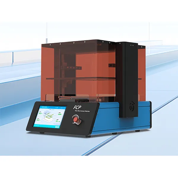
MatMeas FCP Thin Film Corona Polarizer
The MatMeas FCP Thin Film Corona Polarizer is an advanced laboratory platform specifically engineered for high-efficiency polarization of piezoelectric polymer films (e.g., PVDF, P(VDF-TrFE)). Delivering 0 to −30 kV / 2 mA negative corona discharge across a spacious 200 mm × 200 mm active poling area, it features dual independent power modules to eliminate electrical cross-talk and utilizes an innovative non-contact single-wire electrode fixture. With optional FCPHT150 high-temperature heating stage (≤ 150°C, precision ≤ ±3°C) and FCPOP01 smart suite supporting remote OTA updates and API integration, the FCP uniformly polarizes ultra-thin films (5 μm to 200 μm, ideally 10–50 μm) from custom coupons (e.g., 50 mm × 50 mm) up to 200 mm × 200 mm sheets without dielectric breakdown.
View details →
MatMeas SPD20KVPOS Air Corona High Voltage Polarization Device
The MatMeas SPD20KVPOS is an intelligent, highly compact Air High-Voltage Polarization Device engineered specifically for the efficient corona poling of piezoelectric ceramic thin films and bulk materials. Delivering up to 20kV of polarization voltage and offering PID precision temperature control up to 180°C, this desktop system is perfectly optimized for both laboratory R&D and educational environments. It features a proprietary visual monitoring interface for real-time tracking of polarization states, combined with one-click operation. Designed with uncompromising safety, it integrates isolation shielding technology, mechanical safety interlocks, and an independent breakdown alarm system, making it the ultimate tool for safely mastering advanced piezoelectric polarization techniques.
View details →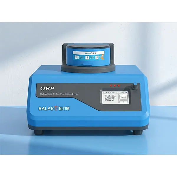
MatMeas OBP Series High Voltage Piezoelectric Ceramic Polarization
MatMeas OBP Series High Voltage Piezoelectric Ceramic Polarization Instrument is a compact, precise lab device designed for bulk and thin-film materials. It helps achieve optimal polarization effects through process optimization.
View details →Request High-Precision Testing Solutions
Get expert guidance and customized instruments for your functional materials project.